- 您现在的位置:买卖IC网 > PDF目录19897 > ADM1073ARUZ-REEL7 (Analog Devices Inc)IC CTRLR HOTSWAP -48V 14TSSOP PDF资料下载
参数资料
| 型号: | ADM1073ARUZ-REEL7 |
| 厂商: | Analog Devices Inc |
| 文件页数: | 16/24页 |
| 文件大小: | 370K |
| 描述: | IC CTRLR HOTSWAP -48V 14TSSOP |
| 产品培训模块: | Hot Swap Design |
| 标准包装: | 1,000 |
| 类型: | 热交换控制器 |
| 应用: | 通用 |
| 内部开关: | 无 |
| 电源电压: | -35 V ~ -80 V |
| 工作温度: | -40°C ~ 85°C |
| 安装类型: | 表面贴装 |
| 封装/外壳: | 14-TSSOP(0.173",4.40mm 宽) |
| 供应商设备封装: | 14-TSSOP |
| 包装: | 带卷 (TR) |
| 配用: | EVAL-ADM1073MEBZ-ND - BOARD EVALUATION FOR ADM1073 |
ADM1073
Data Sheet
Rev. B | Page 16 of 24
DRAIN
Analog input fed by a resistor connected to the drain of the
FET. This pin is clamped to go no higher than 4 V with respect
to VEE. Below this level, the voltage on the pin is monitored so
that, if it falls below 2 V, the PWRGD
output can be set. Above
the 4 V level, the current into the pin is detected and used to
modulate the maximum on-time for the linear FET driver. This
is done by summing a proportion of the drain input current
with the charging current for the TIMER timing capacitor,
thereby reducing the allowable on-time.
PWRGD
Output to indicate when the load capacitor is fully charged.
This is an open collector output with internal pull-up to V
IN
.
When a normal startup is initiated, the PWRGD
output is
latched low when the DRAIN pin falls below 2 V. The latch is
reset, if either the input supply goes out of range or a current
limit time-out event occurs. The second of these cases ensures
that, if a voltage step of greater than 2 V is presented at the
input, the
PWRGD
flag does not go high while the load
capacitor is being charged up to the additional voltage.
LATCHED
Output to indicate when the device has completed the maxi-
mum number (7) of PWM cycles. This is an open collector
output with an internal current source pull-up. If this PWM
time-out event occurs, the GATE pin is latched low and the
LATCHED
output is set low. This condition can then be reset
by either a power cycling event or a low signal to either the
SHDN
input or the RESTART
input. By connecting the
LATCHED
signal directly to SHDN
, the device can effectively
be put into a continuous PWM mode. By connecting the
LATCHED
signal directly to
RESTART
, the device can
effectively be put into autoretry mode, with a 5-second cooling
period.
SPLYGD
Output to indicate when the input supply is within the pro-
grammed voltage window. This is an open collector output with
an internal pull-up current source. For very large capacitive
loads where multiple FETs and controllers are required to meet
the inrush requirements, this output can be used to drive
directly into the UV pin of a second controller. This allows the
second FET to start 1 ms after the first one, with the added
advantage that the input supply UV detection is done on one
controller only. The
SPLYGD
output is asserted only when the
ADM1073 is not in reset mode.
RESTART
Edge-triggered input. Allows the user to remotely command a
5-second shutdown and restart of the hot swap function,
effectively simulating a board removal and replacement. The
shutdown function is triggered by a low pulse of at least 5 祍 at
the pin. This pin has an internal pull-up of approximately 6 礎,
allowing it to be driven by an open collector pull-down output
or a push-pull output. The input threshold is 1.5 V.
SHDN
Level-triggered input. Allows the user to command a shutdown
of the hot swap function. When this input is set low, the GATE
output is switched to V
EE
to turn the FET off. This pin has an
internal pull-up of approximately 6 礎, allowing it to be driven
by an open collector pull-down output or a push-pull output.
The input threshold is 1.5 V.
UNDERVOLTAGE/OVERVOLTAGE DETECTION
The ADM1073 incorporates dual pin undervoltage and
overvoltage detection, with a programmable operating voltage
window. When the voltage on the UV pin falls below the UV
falling threshold or the voltage on the OV pin rises above the
OV rising threshold, a fault signal is generated that disables the
linear current regulator and results in the GATE pin being
pulled low. The voltage fault signal is time filtered so that faults
of a duration less than the UV glitch filter time (0.6 ms) and OV
glitch filter time (5 祍) do not force the gate drive low. The filter
operates only on the faulting edge, that is, on a high-to-low
transition on the undervoltage monitor and on a low-to-high
transition on the overvoltage monitor.
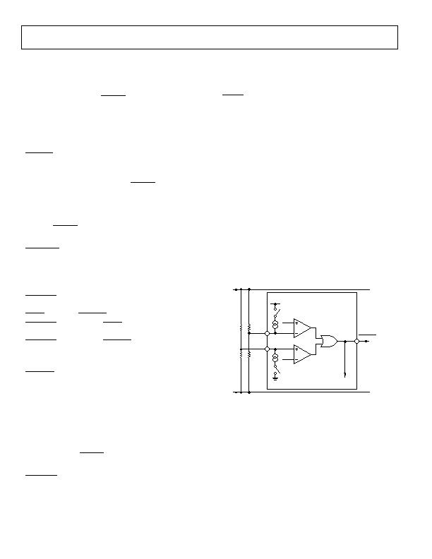
1.93V
868mV
UNDERVOLTAGE
DETECTOR
OVERVOLTAGE
DETECTOR
ADM1073
FET DRIVE
ENABLE
SPLYGD
48V RTN
48V IN
R4
R3
2
1
OV
UV
V
IN
Figure 33. Undervoltage and Overvoltage Circuitry
(Standard 4-Resistor Configuration)
The operating voltage window is determined by selecting the
resistor ratios R1/R2 and R3/R4. These resistor networks form
two resistor dividers that generate the voltages at the UV and
OV pins, which are proportional to the supply voltage. By
choosing these ratios carefully, the user can program the
ADM1073 to apply the supply voltage to the load only when it is
within specific thresholds. Note that 1% tolerance resistors
should always be used to maintain the accuracy of the pro-
grammed thresholds.
相关PDF资料 |
PDF描述 |
|---|---|
| R0.5Z-0505/HP | CONV DC/DC 0.5W 05VIN 05VOUT |
| RMM30DTBT | CONN EDGECARD 60POS R/A .156 SLD |
| V110B5H100BL | CONVERTER MOD DC/DC 5V 100W |
| GEM18DRYH-S13 | CONN EDGECARD 36POS .156 EXTEND |
| NCV8509PDW26G | IC REG LDO 5V/2.6V 16-SOIC |
相关代理商/技术参数 |
参数描述 |
|---|---|
| ADM1073BRUZ | 功能描述:IC CTRLR HOTSWAP -48V 14TSSOP 制造商:analog devices inc. 系列:* 零件状态:上次购买时间 标准包装:1 |
| ADM1073BRUZ-REEL7 | 功能描述:IC CTRLR HOTSWAP -48V 14TSSOP 制造商:analog devices inc. 系列:* 零件状态:上次购买时间 标准包装:1 |
| ADM1075 | 制造商:AD 制造商全称:Analog Devices 功能描述:?48 V Hot Swap Controller and Digital |
| ADM1075-1ACPZ | 功能描述:IC HOT SWAP CTRLR -48V 28LFCSP RoHS:是 类别:集成电路 (IC) >> PMIC - 热交换 系列:- 产品培训模块:Lead (SnPb) Finish for COTS Obsolescence Mitigation Program 标准包装:119 系列:- 类型:热交换控制器 应用:通用型,PCI Express? 内部开关:无 电流限制:- 电源电压:3.3V,12V 工作温度:-40°C ~ 85°C 安装类型:表面贴装 封装/外壳:80-TQFP 供应商设备封装:80-TQFP(12x12) 包装:托盘 产品目录页面:1423 (CN2011-ZH PDF) |
| ADM1075-1ACPZ-RL7 | 功能描述:IC HOT SWAP CTRLR -48V 28LFCSP RoHS:是 类别:集成电路 (IC) >> PMIC - 热交换 系列:- 产品培训模块:Lead (SnPb) Finish for COTS Obsolescence Mitigation Program 标准包装:119 系列:- 类型:热交换控制器 应用:通用型,PCI Express? 内部开关:无 电流限制:- 电源电压:3.3V,12V 工作温度:-40°C ~ 85°C 安装类型:表面贴装 封装/外壳:80-TQFP 供应商设备封装:80-TQFP(12x12) 包装:托盘 产品目录页面:1423 (CN2011-ZH PDF) |
发布紧急采购,3分钟左右您将得到回复。