- 您现在的位置:买卖IC网 > PDF目录10157 > ADM3311EARS-REEL (Analog Devices Inc)IC TXRX RS-232 3:5 2.7V 28SSOP PDF资料下载
参数资料
| 型号: | ADM3311EARS-REEL |
| 厂商: | Analog Devices Inc |
| 文件页数: | 7/24页 |
| 文件大小: | 0K |
| 描述: | IC TXRX RS-232 3:5 2.7V 28SSOP |
| 标准包装: | 1 |
| 类型: | 收发器 |
| 驱动器/接收器数: | 3/5 |
| 规程: | RS232 |
| 电源电压: | 2.7 V ~ 3.6 V |
| 安装类型: | 表面贴装 |
| 封装/外壳: | 28-SSOP(0.209",5.30mm 宽) |
| 供应商设备封装: | 28-SSOP |
| 包装: | 标准包装 |
| 其它名称: | ADM3311EARSREEDKR |
Data Sheet
ADM3307E/ADM3310E/ADM3311E/ADM3312E/ADM3315E
Rev. I | Page 15 of 24
Transmitter (Driver) Section
The drivers convert 3.3 V logic input levels into EIA-232 output
levels. With VCC = 3.0 V and driving an EIA-232 load, the
output voltage swing is typically ±6.4 V (or ±5.5 V for
ADM3310E and ADM3315E).
Unused inputs may be left unconnected, because an internal
400 kV pull-up resistor pulls them high forcing the outputs into
a low state. The input pull-up resistors typically source 8 mA
when grounded, so unused inputs should either be connected to
VCC or left unconnected in order to minimize power
consumption.
Receiver Section
The receivers are inverting level shifters that accept RS-232
input levels and translate them into 3.3 V logic output levels.
The inputs have internal 5 kΩ pull-down resistors (22 kΩ for
the ADM3310E) to ground and are also protected against
overvoltages of up to ±30 V. Unconnected inputs are pulled to
0 V by the internal 5 kΩ (or 22 kΩ for the ADM3315E) pull-
down resistor. This, therefore, results in a Logic 1 output level
for unconnected inputs or for inputs connected to GND.
The receivers have Schmitt trigger inputs with a hysteresis level
of 0.14 V. This ensures error-free reception for both noisy
inputs and for inputs with slow transition times.
ENABLE AND SHUTDOWN
The enable function is intended to facilitate data bus
connections where it is desirable to three-state the receiver
outputs. In the disabled mode, all receiver outputs are placed in
a high impedance state. The shutdown function is intended to
shut the device down, thereby minimizing the quiescent
current. In shutdown, all transmitters are disabled. All receivers
are shut down, except for Receiver R3 (ADM3307E,
ADM3312E, and ADM3315E), Receiver R5 (ADM3311E), and
Receiver R4 and Receiver R5 (ADM3310E). Note that disabled
transmitters are not three-stated in shutdown, so it is not
permitted to connect multiple (RS-232) driver outputs together.
The shutdown feature is very useful in battery-operated systems
because it reduces the power consumption to 66 nW. During
shutdown, the charge pump is also disabled. When exiting
shutdown, the charge pump is restarted and it takes
approximately 100 μs for it to reach its steady-state operating
conditions.
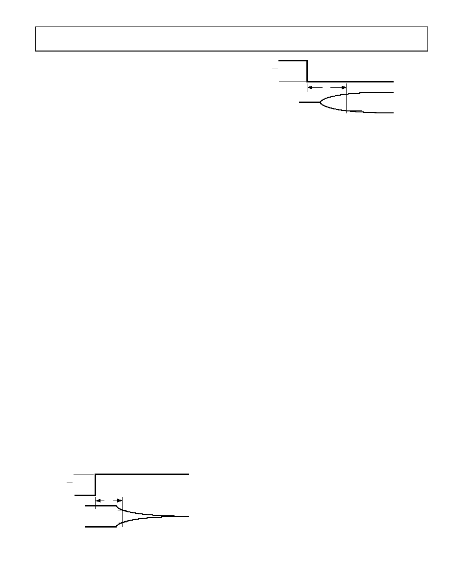
0V
3V
EN INPUT
tDR
VOH –0.1V
VOL +0.1V
VOH
VOL
RECEIVER
OUTPUT
0
29
15
-0
28
Figure 28. Receiver Disable Timing
3V
0.4V
0V
3V
tER
EN INPUT
VOH
VOL
RECEIVER
OUTPUT
02
91
5-
02
9
Figure 29. Receiver Enable Timing
High Baud Rate
The ADM33xxE features high slew rates, permitting data
transmission at rates well in excess of the EIA/RS-232E
specifications. RS-232 voltage levels are maintained at data rates
up to 230 kbps (460 kbps for ADM3307E) under worst-case
loading conditions. This allows for high speed data links
between two terminals.
LAYOUT AND SUPPLY DECOUPLING
Because of the high frequencies at which the ADM33xxE
oscillator operates, particular care should be taken with printed
circuit board layout, with all traces being as short as possible
and C1 to C3 being connected as close to the device as possible.
The use of a ground plane under and around the device is also
highly recommended.
When the oscillator starts up during Green Idle operation, large
current pulses are taken from VCC. For this reason, VCC should
be decoupled with a parallel combination of 10 μF tantalum and
0.1 μF ceramic capacitors, mounted as close to the VCC pin as
possible.
Capacitor C1 to Capacitor C3 can have values between 0.1 μF and 1
μF. Larger values give lower ripple. These capacitors can be either
electrolytic capacitors chosen for low equivalent series resistance
(ESR) or nonpolarized types, but the use of ceramic types is highly
recommended. If polarized electrolytic capacitors are used, polarity
must be observed (as shown by C1+).
ESD/EFT TRANSIENT PROTECTION SCHEME
The ADM33xxE uses protective clamping structures on all inputs
and outputs that clamp the voltage to a safe level and dissipate the
energy present in ESD (electrostatic) and EFT (electrical fast
transients) discharges. A simplified schematic of the protection
Figure 33 for ADM3307E protection structure).
Each input and output contains two back-to-back high speed
clamping diodes. During normal operation with maximum RS-232
signal levels, the diodes have no effect as one or the other is reverse
biased depending on the polarity of the signal. If, however, the
voltage exceeds about ±50 V, reverse breakdown occurs and the
voltage is clamped at this level. The diodes are large p-n junctions
designed to handle the instantaneous current surge that can exceed
several amperes.
相关PDF资料 |
PDF描述 |
|---|---|
| VE-B5Y-MW | CONVERTER MOD DC/DC 3.3V 66W |
| VI-BNY-MV-F4 | CONVERTER MOD DC/DC 3.3V 99W |
| LTC1605-1IG | IC A/D CONV 16BIT SAMPLNG 28SSOP |
| VI-BNY-MV-F3 | CONVERTER MOD DC/DC 3.3V 99W |
| EXP-0921/02/S | CONN RCPT 2POS IP68 W/SOCKETS |
相关代理商/技术参数 |
参数描述 |
|---|---|
| ADM3311EARS-REEL2.5 | 制造商:未知厂家 制造商全称:未知厂家 功能描述:Transceiver |
| ADM3311EARS-REEL25 | 制造商:AD 制造商全称:Analog Devices 功能描述:15 kV ESD Protected, +2.7 V to +3.6 V Serial Port Transceiver with Green Idle⑩ |
| ADM3311EARS-REEL7 | 功能描述:IC TXRX RS-232 3:5 2.7V 28SSOP RoHS:否 类别:集成电路 (IC) >> 接口 - 驱动器,接收器,收发器 系列:- 标准包装:121 系列:- 类型:收发器 驱动器/接收器数:1/1 规程:RS422,RS485 电源电压:3 V ~ 3.6 V 安装类型:表面贴装 封装/外壳:10-WFDFN 裸露焊盘 供应商设备封装:10-DFN(3x3) 包装:管件 |
| ADM3311EARSZ | 功能描述:IC TXRX RS-232 3:5 2.7V 28SSOP RoHS:是 类别:集成电路 (IC) >> 接口 - 驱动器,接收器,收发器 系列:- 产品培训模块:RS-232 & USB Transceiver 标准包装:2,000 系列:- 类型:收发器 驱动器/接收器数:1/1 规程:RS232 电源电压:3 V ~ 5.5 V 安装类型:表面贴装 封装/外壳:16-SSOP(0.209",5.30mm 宽) 供应商设备封装:16-SSOP 包装:带卷 (TR) 其它名称:296-19849-2 |
| ADM3311EARSZ-REEL | 功能描述:IC TXRX RS232 3:5 2.7V 28SSOP RoHS:是 类别:集成电路 (IC) >> 接口 - 驱动器,接收器,收发器 系列:- 标准包装:98 系列:* |
发布紧急采购,3分钟左右您将得到回复。