- 您现在的位置:买卖IC网 > PDF目录10157 > ADM3311EARS-REEL (Analog Devices Inc)IC TXRX RS-232 3:5 2.7V 28SSOP PDF资料下载
参数资料
| 型号: | ADM3311EARS-REEL |
| 厂商: | Analog Devices Inc |
| 文件页数: | 8/24页 |
| 文件大小: | 0K |
| 描述: | IC TXRX RS-232 3:5 2.7V 28SSOP |
| 标准包装: | 1 |
| 类型: | 收发器 |
| 驱动器/接收器数: | 3/5 |
| 规程: | RS232 |
| 电源电压: | 2.7 V ~ 3.6 V |
| 安装类型: | 表面贴装 |
| 封装/外壳: | 28-SSOP(0.209",5.30mm 宽) |
| 供应商设备封装: | 28-SSOP |
| 包装: | 标准包装 |
| 其它名称: | ADM3311EARSREEDKR |
ADM3307E/ADM3310E/ADM3311E/ADM3312E/ADM3315E
Data Sheet
Rev. I | Page 16 of 24
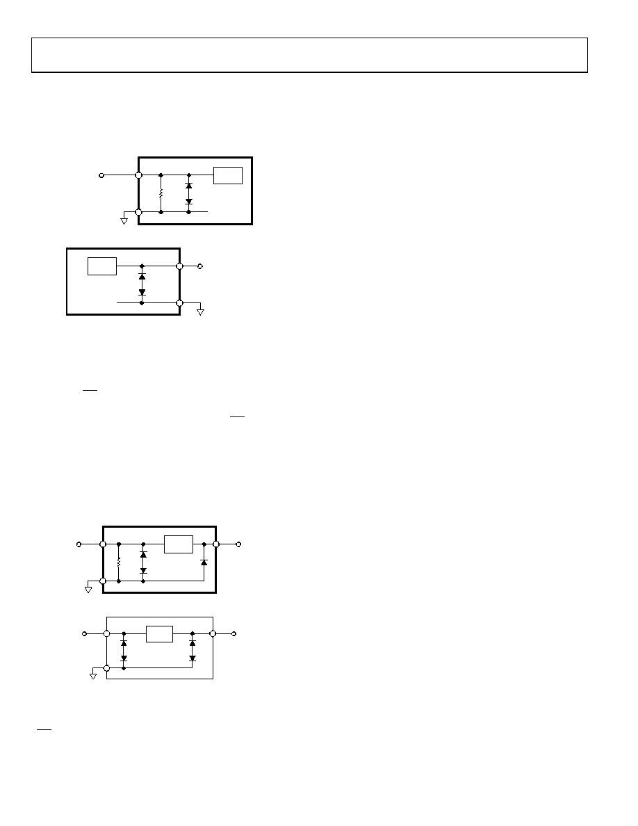
The transmitter outputs and receiver inputs have a similar
protection structure. The receiver inputs can also dissipate some
of the energy through the internal 5 k (or 22 k for the
ADM3310E) resistor to GND as well as through the protection
diodes.
RIN
Rx
D1
D2
RECEIVER
INPUT
02915-
030
Figure 30. Receiver Input Protection Scheme
Tx
D1
D2
TRANSMITTER
OUTPUT
02915-
031
Figure 31. Transmitter Output Protection Scheme
The ADM3307E protection scheme is slightly different (see
Figure 32 and Figure 33). The receiver inputs, transmitter
inputs, and transmitter outputs contain two back-to-back high
speed clamping diodes. The receiver outputs (CMOS outputs),
the SD and EN pins, contain a single reverse biased high speed
clamping diode. Under normal operation with maximum
CMOS signal levels, the receiver output, SD, and EN protection
diodes have no effect because they are reversed biased. If,
however, the voltage exceeds about 15 V, reverse breakdown
occurs and the voltage is clamped at this level. If the voltage
reaches 0.7 V, the diode is forward biased and the voltage is
clamped at this level. The receiver inputs can also dissipate
some of the energy through the internal 5 k resistor to GND
as well as through the protection diodes.
RIN
D1
D3
D2
RECEIVER
INPUT
RECEIVER
OUTPUT
Rx
02915-
032
Figure 32. ADM3307E Receiver Input Protection Scheme
D1
D2
D3
D4
TRANSMITTER
OUTPUT
TRANSMITTER
INPUT
Tx
02915-
033
Figure 33. ADM3307E Transmitter Output Protection Scheme
The protection structures achieve ESD protection up to ±15 kV
on all RS-232 I/O lines (and all CMOS lines, including SD and
EN for the ADM3307E). For methods used to test the
protection scheme, see the ESD Testing (IEC 1000-4-2) section.
ESD TESTING (IEC 1000-4-2)
IEC 1000-4-2 (previously 801-2) specifies compliance testing
using two coupling methods, contact discharge and air-gap
discharge. Contact discharge calls for a direct connection to the
unit being tested. Airgap discharge uses a higher test voltage but
does not make direct contact with the unit under testing. With
air discharge, the discharge gun is moved toward the unit under
testing, which develops an arc across the air gap, thus the term
air discharge. This method is influenced by humidity,
temperature, barometric pressure, distance, and rate of closure
of the discharge gun. The contact discharge method, while less
realistic, is more repeatable and is gaining acceptance in
preference to the air-gap method.
Although very little energy is contained within an ESD pulse,
the extremely fast rise time coupled with high voltages can
cause failures in unprotected semiconductors. Catastrophic
destruction can occur immediately as a result of arcing or
heating. Even if catastrophic failure does not occur immediately,
the device can suffer from parametric degradation that can
result in degraded performance. The cumulative effects of
continuous exposure can eventually lead to complete failure.
I/O lines are particularly vulnerable to ESD damage. Simply
touching or plugging in an I/O cable can result in a static
discharge that can damage or completely destroy the interface
product connected to the I/O port. Traditional ESD test
methods, such as the MIL-STD-883B method 3015.7, do not
fully test a product’s susceptibility to this type of discharge. This
test was intended to test a product’s susceptibility to ESD
damage during handling.
Each pin is tested with respect to all other pins. There are some
important differences between the traditional test and the IEC
test.
The IEC test is much more stringent in terms of discharge
energy. The peak current injected is over four times greater.
The current rise time is significantly faster in the IEC test.
The IEC test is carried out while power is applied to the
device.
It is possible that the ESD discharge could induce latch-up in
the device under test. This test, therefore, is more representative
of a real world I/O discharge where the equipment is operating
normally with power applied. For maximum peace of mind,
however, both tests should be performed, ensuring maximum
protection both during handling and later during field service.
相关PDF资料 |
PDF描述 |
|---|---|
| VE-B5Y-MW | CONVERTER MOD DC/DC 3.3V 66W |
| VI-BNY-MV-F4 | CONVERTER MOD DC/DC 3.3V 99W |
| LTC1605-1IG | IC A/D CONV 16BIT SAMPLNG 28SSOP |
| VI-BNY-MV-F3 | CONVERTER MOD DC/DC 3.3V 99W |
| EXP-0921/02/S | CONN RCPT 2POS IP68 W/SOCKETS |
相关代理商/技术参数 |
参数描述 |
|---|---|
| ADM3311EARS-REEL2.5 | 制造商:未知厂家 制造商全称:未知厂家 功能描述:Transceiver |
| ADM3311EARS-REEL25 | 制造商:AD 制造商全称:Analog Devices 功能描述:15 kV ESD Protected, +2.7 V to +3.6 V Serial Port Transceiver with Green Idle⑩ |
| ADM3311EARS-REEL7 | 功能描述:IC TXRX RS-232 3:5 2.7V 28SSOP RoHS:否 类别:集成电路 (IC) >> 接口 - 驱动器,接收器,收发器 系列:- 标准包装:121 系列:- 类型:收发器 驱动器/接收器数:1/1 规程:RS422,RS485 电源电压:3 V ~ 3.6 V 安装类型:表面贴装 封装/外壳:10-WFDFN 裸露焊盘 供应商设备封装:10-DFN(3x3) 包装:管件 |
| ADM3311EARSZ | 功能描述:IC TXRX RS-232 3:5 2.7V 28SSOP RoHS:是 类别:集成电路 (IC) >> 接口 - 驱动器,接收器,收发器 系列:- 产品培训模块:RS-232 & USB Transceiver 标准包装:2,000 系列:- 类型:收发器 驱动器/接收器数:1/1 规程:RS232 电源电压:3 V ~ 5.5 V 安装类型:表面贴装 封装/外壳:16-SSOP(0.209",5.30mm 宽) 供应商设备封装:16-SSOP 包装:带卷 (TR) 其它名称:296-19849-2 |
| ADM3311EARSZ-REEL | 功能描述:IC TXRX RS232 3:5 2.7V 28SSOP RoHS:是 类别:集成电路 (IC) >> 接口 - 驱动器,接收器,收发器 系列:- 标准包装:98 系列:* |
发布紧急采购,3分钟左右您将得到回复。