- 您现在的位置:买卖IC网 > PDF目录9663 > ADN2806ACPZ-500RL7 (Analog Devices Inc)IC CLK/DATA REC 622MBPS 32-LFCSP PDF资料下载
参数资料
| 型号: | ADN2806ACPZ-500RL7 |
| 厂商: | Analog Devices Inc |
| 文件页数: | 7/20页 |
| 文件大小: | 0K |
| 描述: | IC CLK/DATA REC 622MBPS 32-LFCSP |
| 标准包装: | 500 |
| 类型: | 时钟和数据恢复(CDR),多路复用器 |
| PLL: | 是 |
| 主要目的: | SONET/SDH |
| 输入: | CML |
| 输出: | LVDS |
| 电路数: | 1 |
| 比率 - 输入:输出: | 1:2 |
| 差分 - 输入:输出: | 是/是 |
| 频率 - 最大: | 622MHz |
| 电源电压: | 3 V ~ 3.6 V |
| 工作温度: | -40°C ~ 85°C |
| 安装类型: | 表面贴装 |
| 封装/外壳: | 32-VFQFN 裸露焊盘,CSP |
| 供应商设备封装: | 32-LFCSP-VQ(5x5) |
| 包装: | 带卷 (TR) |
ADN2806
Rev. C | Page 15 of 20
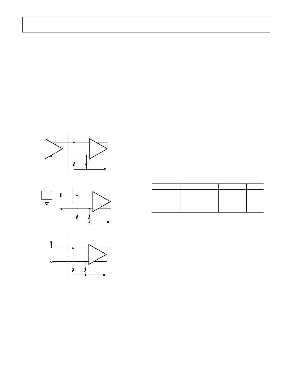
REFERENCE CLOCK (OPTIONAL)
A reference clock is not required to perform clock and data
recovery with the ADN2806; however, support for an optional
reference clock is provided. The reference clock can be driven
differentially or in a single-ended fashion. If the reference
clock is not being used, REFCLKP should be tied to VCC, and
REFCLKN can be left floating or tied to VEE (the inputs are
for sample configurations.
The REFCLK input buffer accepts any differential signal with a
peak-to-peak differential amplitude of greater than 100 mV (for
example, LVPECL or LVDS) or a standard single-ended, low
voltage TTL input, providing maximum system flexibility.
Phase noise and duty cycle of the reference clock are not
critical, and 100 ppm accuracy is sufficient.
100k
VCC/2
100k
ADN2806
REFCLKP
10
11
REFCLKN
BUFFER
0
58
31
-0
21
Figure 16. Differential REFCLK Configuration
100k
VCC/2
100k
ADN2806
REFCLKP
OUT
REFCLKN
BUFFER
VCC
CLK
OSC
0
58
31
-0
22
Figure 17. Single-Ended REFCLK Configuration
100k
VCC/2
100k
ADN2806
REFCLKP
10
11
NC
REFCLKN
BUFFER
VCC
0
58
31
-0
23
Figure 18. No REFCLK Configuration
There are two mutually exclusive uses, or modes, of the
reference clock. The reference clock can be used either to help
the ADN2806 lock onto data or to measure the frequency of the
incoming data to within 0.01%. The modes are mutually
exclusive because in the first use the user knows exactly what
the data rate is and wants to force the part to lock onto only that
data rate, and in the second use the user does not know what
the data rate is and wants to measure it.
Lock-to-reference mode is enabled by writing a 1 to I2C Register
Bit CTRLA[0]. Fine data rate readback mode is enabled by
writing a 1 to I2C Register Bit CTRLA[1]. Writing a 1 to both of
these bits at the same time causes an indeterminate state and is
not supported.
Using the Reference Clock to Lock onto Data
In this mode, the ADN2806 locks onto a frequency derived
from the reference clock according to
Data Rate/2CTRLA[5:2] = REFCLK/2CTRLA[7, 6]
The user must provide a reference clock that is a function of the
data rate. By default, the ADN2806 expects a reference clock of
19.44 MHz. Other options are 38.88 MHz, 77.76 MHz, and
155.52 MHz, which are selected by programming CTRLA[7, 6].
CTRLA[5:2] should be programmed to [0101] for all cases.
Table 11. CTRLA Settings
CTRLA[7, 6]
Range (MHz)
CTRLA[5:2]
Ratio
00
19.44
0101
25
01
38.88
0101
25
10
77.76
0101
25
11
155.52
0101
25
For example, if the reference clock frequency is 38.88 MHz and the
input data rate is 622.08 Mbps, CTRLA[7, 6] is set to [01] to
produce a divided-down reference clock of 19.44 MHz, and
CTRLA[5:2] is set to [0101], that is, 5, because
622.08 Mbps/19.44 MHz = 25
In this mode, if the ADN2806 loses lock for any reason, it relocks
onto the reference clock and continues to output a stable clock.
While the ADN2806 is operating in lock-to-reference mode,
a 0 to 1 transition should be written into the CTRLA[0] bit to
initiate a lock-to-reference clock command.
相关PDF资料 |
PDF描述 |
|---|---|
| CS3101A-32-22S | CONN RCPT 54POS IN LINE W/SCKT |
| VE-JTX-MX-F3 | CONVERTER MOD DC/DC 5.2V 75W |
| VE-JTX-MX-F2 | CONVERTER MOD DC/DC 5.2V 75W |
| VE-JTW-MX-F4 | CONVERTER MOD DC/DC 5.5V 75W |
| ADN2804ACPZ-RL7 | IC CLK/DATA REC 622MBPS 32-LFCSP |
相关代理商/技术参数 |
参数描述 |
|---|---|
| ADN2806ACPZ-RL7 | 功能描述:IC CLK/DATA REC 622MBPS 32-LFCSP RoHS:是 类别:集成电路 (IC) >> 时钟/计时 - 专用 系列:- 标准包装:28 系列:- 类型:时钟/频率发生器 PLL:是 主要目的:Intel CPU 服务器 输入:时钟 输出:LVCMOS 电路数:1 比率 - 输入:输出:3:22 差分 - 输入:输出:无/是 频率 - 最大:400MHz 电源电压:3.135 V ~ 3.465 V 工作温度:0°C ~ 85°C 安装类型:表面贴装 封装/外壳:64-TFSOP (0.240",6.10mm 宽) 供应商设备封装:64-TSSOP 包装:管件 |
| ADN2807 | 制造商:AD 制造商全称:Analog Devices 功能描述:155/622 Mb/s Clock and Data Recovery IC with Integrated Limiting Amp |
| ADN2807ACP | 制造商:Analog Devices 功能描述:CDR 155.52Mbps/166.63Mbps/622.08Mbps/666.51Mbps SONET/SDH 48-Pin LFCSP EP Tray |
| ADN2807ACP-RL | 制造商:AD 制造商全称:Analog Devices 功能描述:155/622 Mb/s Clock and Data Recovery IC with Integrated Limiting Amp |
| ADN2807ACPZ | 功能描述:IC CLOCK/DATA RECOVERY 48LFCSP RoHS:是 类别:集成电路 (IC) >> 时钟/计时 - 专用 系列:- 标准包装:28 系列:- 类型:时钟/频率发生器 PLL:是 主要目的:Intel CPU 服务器 输入:时钟 输出:LVCMOS 电路数:1 比率 - 输入:输出:3:22 差分 - 输入:输出:无/是 频率 - 最大:400MHz 电源电压:3.135 V ~ 3.465 V 工作温度:0°C ~ 85°C 安装类型:表面贴装 封装/外壳:64-TFSOP (0.240",6.10mm 宽) 供应商设备封装:64-TSSOP 包装:管件 |
发布紧急采购,3分钟左右您将得到回复。