参数资料
| 型号: | ADN2890ACP-RL7 |
| 厂商: | Analog Devices Inc |
| 文件页数: | 12/12页 |
| 文件大小: | 0K |
| 描述: | IC AMP LIM 16LFCSP |
| 产品变化通告: | Product Discontinuance 27/July/2010 |
| 标准包装: | 1 |
| 放大器类型: | 限制 |
| 电路数: | 1 |
| 输出类型: | 差分 |
| 电压 - 输入偏移: | 100µV |
| 电流 - 电源: | 39mA |
| 电压 - 电源,单路/双路(±): | 3 V ~ 3.6 V |
| 工作温度: | -40°C ~ 85°C |
| 安装类型: | 表面贴装 |
| 封装/外壳: | 16-VFQFN 裸露焊盘,CSP |
| 供应商设备封装: | 16-LFCSP-VQ |
| 包装: | 剪切带 (CT) |
| 其它名称: | ADN2890ACP-RL7CT |
Data Sheet
ADN2890
Rev. A | Page 9 of 12
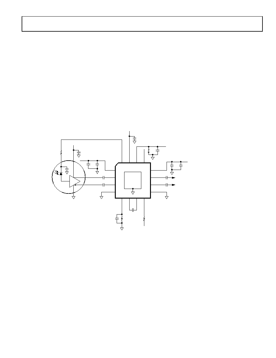
APPLICATIONS INFORMATION
PCB DESIGN GUIDELINES
Proper RF PCB design techniques must be used for optimal
performance.
Power Supply Connections and Ground Planes
Use of one low impedance ground plane is recommended. The
VEE pins should be soldered directly to the ground plane to
reduce series inductance. If the ground plane is an internal
plane and connections to the ground plane are made through
vias, multiple vias can be used in parallel to reduce the series
inductance, especially on Pin 9, which is the ground return for
the output buffers. The exposed pad should be connected to the
GND plane using filled vias so that solder does not leak through
the vias during reflow. Using filled vias under the package
greatly enhances the reliability of the connectivity of the
exposed pad to the GND plane during reflow.
Use of a 10 F electrolytic capacitor between VCC and VEE is
recommended at the location where the 3.3 V supply enters the
PCB. When using 0.1 F and 1 nF ceramic chip capacitors, they
should be placed between the IC power supply VCC and VEE,
as close as possible to the ADN2890 VCC pins.
If connections to the supply and ground are made through vias,
the use of multiple vias in parallel helps to reduce series
inductance, especially on Pin 12, which supplies power to the
high speed OUTP/OUTN output buffers. Refer to the schematic
in Figure 8 for recommended connections.
Figure 8. Typical ADN2890 Applications Circuit
04509-0-007
CONNECT
EXPOSED
PAD TO
GND
AVCC
1
THRADJ
5
CAZ1
6
CAZ2
7
LOS
8
PD_CATHODE
16
PD_VCC
15
RSSI_OUT
14
SQUELCH
13
PIN
2
NIN
3
AVEE
4
DRVCC
12
OUTN
10
DRVEE
9
OUTP
C4
C3
11
C2
C1
TO HOST
BOARD
C7
C8
VCC
C5
C6
VCC
C11
C12
R2
200
VCC
R3
4.7k
TO 10k
ON HOST BOARD
VCC
ADN2880
0.1
F
VCC
C9
RSSI MEASUREMENT
TO ADC
R1
C10
C1–C4, C11: 0.01
F X5R/X7R DIELECTRIC, 0201 CASE
C5, C7, C9, C10, C12: 0.1
F X5R/X7R DIELECTRIC, 0402 CASE
C6, C8: 1nF X5R/X7R DIELECTRIC, 0201 CASE
相关PDF资料 |
PDF描述 |
|---|---|
| ADN2891ACPZ-500RL7 | IC AMP LIM 16LFCSP |
| ADN2892ACPZ-500RL7 | IC AMP LIM 16LFCSP |
| ADR827BRMZ-REEL7 | IC OPAMP GP R-R 1MHZ LP 10MSOP |
| ADTL084ARZ-REEL7 | IC OPAMP JFET 5MHZ QUAD 14SOIC |
| AFB02512HHA | FAN DC AXIAL 12V 25X10 13000RPM |
相关代理商/技术参数 |
参数描述 |
|---|---|
| ADN2890ACPZ-RL | 功能描述:IC AMP LIM 16LFCSP RoHS:是 类别:集成电路 (IC) >> Linear - Amplifiers - Instrumentation 系列:- 标准包装:50 系列:- 放大器类型:J-FET 电路数:2 输出类型:- 转换速率:13 V/µs 增益带宽积:3MHz -3db带宽:- 电流 - 输入偏压:65pA 电压 - 输入偏移:3000µV 电流 - 电源:1.4mA 电流 - 输出 / 通道:- 电压 - 电源,单路/双路(±):7 V ~ 36 V,±3.5 V ~ 18 V 工作温度:-40°C ~ 85°C 安装类型:通孔 封装/外壳:8-DIP(0.300",7.62mm) 供应商设备封装:8-PDIP 包装:管件 |
| ADN2890ACPZ-RL7 | 功能描述:IC AMP LIM 16LFCSP RoHS:是 类别:集成电路 (IC) >> Linear - Amplifiers - Instrumentation 系列:- 标准包装:50 系列:- 放大器类型:J-FET 电路数:2 输出类型:- 转换速率:13 V/µs 增益带宽积:3MHz -3db带宽:- 电流 - 输入偏压:65pA 电压 - 输入偏移:3000µV 电流 - 电源:1.4mA 电流 - 输出 / 通道:- 电压 - 电源,单路/双路(±):7 V ~ 36 V,±3.5 V ~ 18 V 工作温度:-40°C ~ 85°C 安装类型:通孔 封装/外壳:8-DIP(0.300",7.62mm) 供应商设备封装:8-PDIP 包装:管件 |
| ADN2890XCP | 制造商:Analog Devices 功能描述:- Trays |
| ADN2891 | 制造商:AD 制造商全称:Analog Devices 功能描述:3.3 V, 3.2 Gbps, Limiting Amplifier |
| ADN2891ACP | 制造商:AD 制造商全称:Analog Devices 功能描述:3.3 V, 3.2 Gbps, Limiting Amplifier |
发布紧急采购,3分钟左右您将得到回复。