参数资料
| 型号: | ADN2890ACPZ-RL7 |
| 厂商: | Analog Devices Inc |
| 文件页数: | 1/12页 |
| 文件大小: | 0K |
| 描述: | IC AMP LIM 16LFCSP |
| 标准包装: | 1 |
| 放大器类型: | 限制 |
| 电路数: | 1 |
| 输出类型: | 差分 |
| 电压 - 输入偏移: | 100µV |
| 电流 - 电源: | 39mA |
| 电压 - 电源,单路/双路(±): | 3 V ~ 3.6 V |
| 工作温度: | -40°C ~ 85°C |
| 安装类型: | 表面贴装 |
| 封装/外壳: | 16-VFQFN 裸露焊盘,CSP |
| 供应商设备封装: | 16-LFCSP-VQ |
| 包装: | 标准包装 |
| 产品目录页面: | 788 (CN2011-ZH PDF) |
| 其它名称: | ADN2890ACPZ-RL7DKR |
3.3 V 2.7 Gb/s
Limiting Amplifier
Data Sheet
Rev. A
Information furnished by Analog Devices is believed to be accurate and reliable. However, no
responsibilityisassumedbyAnalogDevicesforitsuse,norforanyinfringementsofpatentsorother
rightsofthirdpartiesthatmayresultfromitsuse.Specificationssubjecttochangewithoutnotice.No
license is granted by implication or otherwise under any patent or patent rights of Analog Devices.
Trademarksandregisteredtrademarksarethepropertyoftheirrespectiveowners.
One Technology Way, P.O. Box 9106, Norwood, MA 02062-9106, U.S.A.
Tel: 781.329.4700
2004–2013 Analog Devices, Inc. All rights reserved.
FEATURES
SFP reference design available
Input sensitivity: 3 mV p-p
80 ps rise/fall times
CML outputs: 700 mV p-p differential
Programmable LOS detector: 2 mV to 13 mV
Rx signal strength indicator (RSSI):
SFF-8472 compliant average power measurement
Single-supply operation: 3.3 V
Low power dissipation: 130 mW
Available in space-saving 3 mm × 3 mm 16-lead LFCSP
APPLICATIONS
SFP/SFF/GBIC optical transceivers
OC-3/12/48, GbE, Fibre Channel receivers
10GBASE-LX4 transceivers
WDM transponders
GENERAL DESCRIPTION
The ADN2890 is a high gain, limiting amplifier optimized for
use in SONET, Gigabit Ethernet (GbE), and Fibre Channel
optical receivers that accept input levels of up to 2.0 V p-p
differential and have 3 mV p-p differential input sensitivity. The
ADN2890 provides the receiver functions of quantization and
loss of signal (LOS) detection. The ADN2890 can easily operate
at up to 3.2 Gb/s to support LX4 transceivers.
The limiting amplifier also measures average received power
based on a direct measurement of the photodiode current with
better than 1 dB of accuracy over the entire input range of the
receiver. This eliminates the need for external average Rx power
detection circuitry in SFF-8472 compliant optical transceivers.
The ADN2890 limiting amplifier operates from a single 3.3 V
supply, has low power dissipation, and is available in a space-
saving 3 mm × 3 mm 16-lead lead frame chip scale package
(LFCSP).
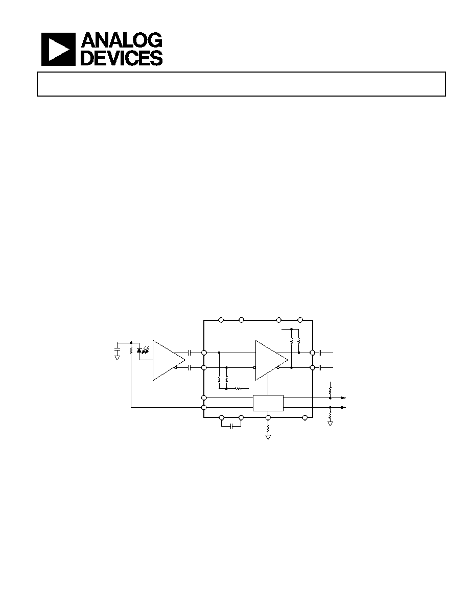
FUNCTIONAL BLOCK DIAGRAM
Figure 1.
04509-0-001
ADN2880
VREF
DRVCC
50
50
50
50
3k
PIN
NIN
PD_VCC
PD_CATHODE
ADN2890
RSSI/LOS
DETECTOR
0.01
F
CAZ1
CAZ2
SQUELCH
AVCC
AVEE
DRVCC
DRVEE
THRADJ
OUTP
LOS
10k
+V
ADuC7020
RSSI_OUT
OUTN
CF
RF
相关PDF资料 |
PDF描述 |
|---|---|
| 0034.6014 | FUSE 1A 250V FAST 4.3MM PCB |
| 0034.6020 | FUSE 4A 250V FAST 4.3MM PCB |
| 0034.6021 | FUSE 5A 250V FAST 4.3MM PCB |
| ADN2892ACPZ-RL | IC AMP LIM 16LFCSP |
| 0034.6018 | FUSE 2.5A 250V FAST 4.3MM PCB |
相关代理商/技术参数 |
参数描述 |
|---|---|
| ADN2890XCP | 制造商:Analog Devices 功能描述:- Trays |
| ADN2891 | 制造商:AD 制造商全称:Analog Devices 功能描述:3.3 V, 3.2 Gbps, Limiting Amplifier |
| ADN2891ACP | 制造商:AD 制造商全称:Analog Devices 功能描述:3.3 V, 3.2 Gbps, Limiting Amplifier |
| ADN2891ACPZ-500RL7 | 功能描述:IC AMP LIM 16LFCSP RoHS:是 类别:集成电路 (IC) >> Linear - Amplifiers - Instrumentation 系列:- 标准包装:1 系列:MicroAmplifier™ 放大器类型:通用 电路数:4 输出类型:- 转换速率:3.5 V/µs 增益带宽积:1MHz -3db带宽:- 电流 - 输入偏压:5pA 电压 - 输入偏移:1500µV 电流 - 电源:220µA 电流 - 输出 / 通道:60mA 电压 - 电源,单路/双路(±):4.5 V ~ 36 V,±2.25 V ~ 18 V 工作温度:-40°C ~ 85°C 安装类型:表面贴装 封装/外壳:14-SOIC(0.154",3.90mm 宽) 供应商设备封装:14-SOIC 包装:剪切带 (CT) 其它名称:296-29363-1 |
| ADN2891ACPZ-RL | 功能描述:IC AMP LIM 16LFCSP RoHS:是 类别:集成电路 (IC) >> Linear - Amplifiers - Instrumentation 系列:- 标准包装:50 系列:- 放大器类型:J-FET 电路数:2 输出类型:- 转换速率:13 V/µs 增益带宽积:3MHz -3db带宽:- 电流 - 输入偏压:65pA 电压 - 输入偏移:3000µV 电流 - 电源:1.4mA 电流 - 输出 / 通道:- 电压 - 电源,单路/双路(±):7 V ~ 36 V,±3.5 V ~ 18 V 工作温度:-40°C ~ 85°C 安装类型:通孔 封装/外壳:8-DIP(0.300",7.62mm) 供应商设备封装:8-PDIP 包装:管件 |
发布紧急采购,3分钟左右您将得到回复。