- 您现在的位置:买卖IC网 > PDF目录11209 > ADN4600ACPZ-R7 (Analog Devices Inc)IC CROSSPOINT SWITCH 8X8 64LFCSP PDF资料下载
参数资料
| 型号: | ADN4600ACPZ-R7 |
| 厂商: | Analog Devices Inc |
| 文件页数: | 8/28页 |
| 文件大小: | 0K |
| 描述: | IC CROSSPOINT SWITCH 8X8 64LFCSP |
| 标准包装: | 1 |
| 系列: | XStream™ |
| 功能: | 交叉点开关 |
| 电路: | 1 x 8:8 |
| 电压电源: | 单电源 |
| 电压 - 电源,单路/双路(±): | 1.7 V ~ 3.6 V |
| 电流 - 电源: | 460mA |
| 工作温度: | -40°C ~ 85°C |
| 安装类型: | 表面贴装 |
| 封装/外壳: | 64-VFQFN 裸露焊盘,CSP |
| 供应商设备封装: | 64-LFCSP-VQ(9x9) |
| 包装: | 标准包装 |
| 其它名称: | ADN4600ACPZ-R7DKR |
第1页第2页第3页第4页第5页第6页第7页当前第8页第9页第10页第11页第12页第13页第14页第15页第16页第17页第18页第19页第20页第21页第22页第23页第24页第25页第26页第27页第28页
ADN4600
Data Sheet
Rev. A | Page 16 of 28
TRANSMITTERS
Output Structure and Output Levels
The ADN4600 transmitter outputs incorporate 50 Ω termination
resistors, ESD protection, and output current switch. Each
channel provides independent control of both the absolute
output level and the pre-emphasis output level. It should be
noted that the choice of output level affects the output common-
mode level. A 600 mV p-p differential output level with full
pre-emphasis range requires an output termination voltage
of 2.5 V or greater; therefore, for the VTTO pin, VCC must be
equal to or greater than 2.5 V.
Pre-Emphasis
The total output amplitude and pre-emphasis setting space is
reduced to a single map of basic settings that provides seven
settings of output equalization to ease programming for typical
channels. The full resolution of seven settings is available through
the I2C interface by writing to Bits[2:0] (the TX PE[2:0] bits) of
the TX[7:0] configuration registers. Table 10 summarizes the
absolute output level, pre-emphasis level, and high frequency
boost for each of the control settings and the typical length of
FR4 trace compensated for by each setting.
Full control of the transmit output levels is available through the
I2C control interface. This full control is achieved by writing to
the TX[7:0] Output Level Control[1:0] registers for the channel
of interest. The supported output levels are shown in Table 12.
The TX[7:0] Output Level Control[1:0] registers must be
programmed to one of the supported settings listed in this table;
other settings are not supported.
The output equalization is optimized for less than 2.5 Gbps
operation, but can be optimized for higher speed applications
up to 4.25 Gbps through the I2C control interface by writing to
the TX DATA RATE bit (Bit 4) of the TX[7:0] configuration
register, with high representing 4.25 Gbps and low representing
2.5 Gbps. The TX[7:0] CTL SRC bit (Bit 7) in the TX[7:0]
Output Level Control 1 register determines whether the pre-
emphasis and output current controls for the channel of interest
are selected from the optimized map or directly from the
TX[7:0] Output Level Control[1:0] registers (per channel).
Setting this bit high selects pre-emphasis control directly from
the TX[7:0] Output Level Control[1:0] registers, and setting it
low selects pre-emphasis control from the optimized map.
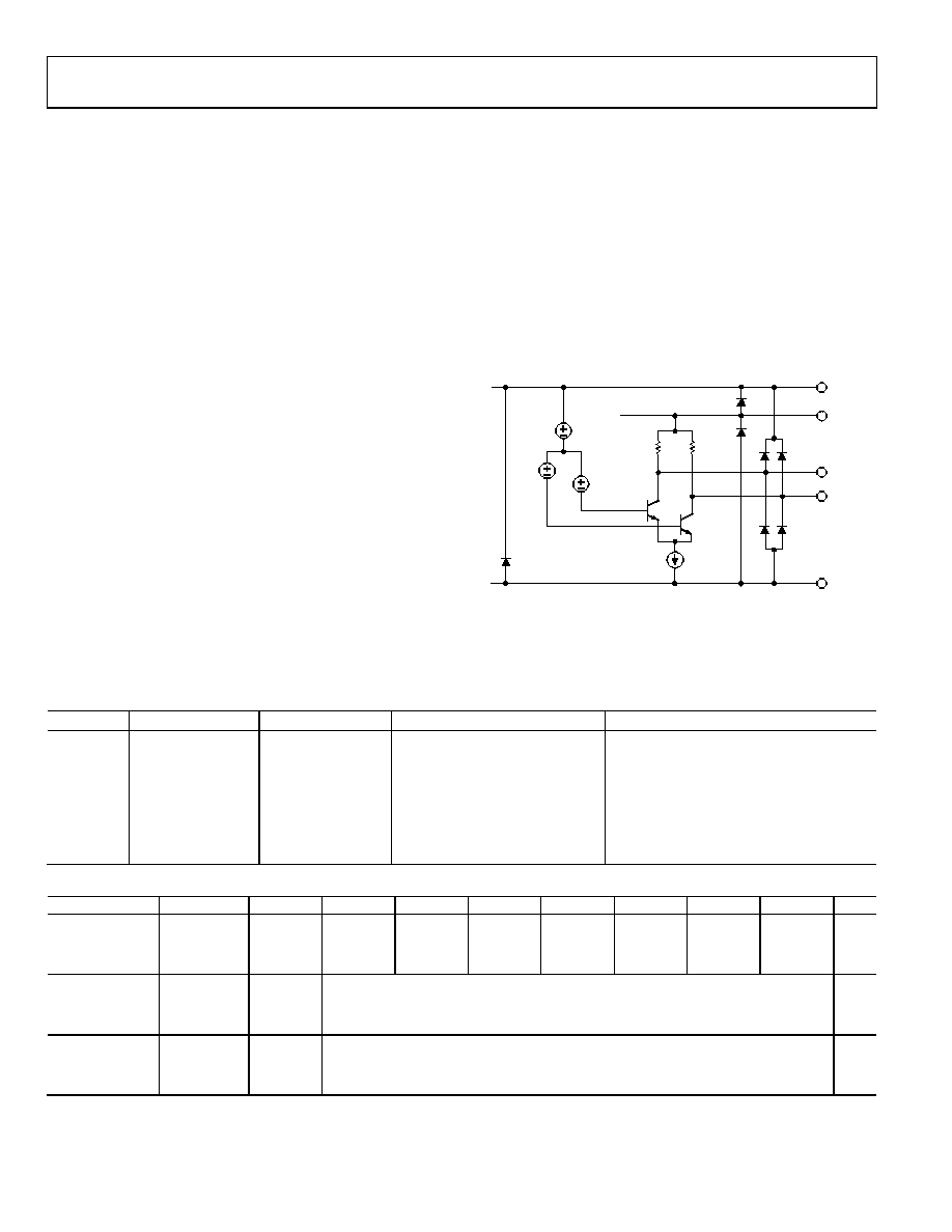
VCC
VTTO
OPx
ONx
VEE
TX SIMPLIFIED DIAGRAM
Q1
Q2
IT
RN
52
RP
52
ON-CHIP
TERMINATION
V3
VC
V2
VP
V1
VN
IDC + TPE
07061-
006
ESD
Figure 29. Simplified Output Structure
Table 10. Transmit Pre-Emphasis Boost and Overshoot vs. Setting
TX PE
Boost (dB)
Overshoot
DC Swing (mV p-p Differential)
Typical FR4 Trace Length (Inches)
0
0%
800
0 to 5
1
2
25%
800
0 to 5
2
3.5
50%
800
10 to 15
3
4.9
75%
800
15 to 20
4
6
100%
800
25 to 30
5
7.4
133%
600
30 to 35
6
9.5
200%
400
35 to 40
Table 11. Transmitters Control Registers
Name
Addr
Bit 7
Bit 6
Bit 5
Bit 4
Bit 3
Bit 2
Bit 1
Bit 0
Def.
TX[7:0]
Configuration
0xE0, 0xE8,
0xF0, 0xF8,
0xD8, 0xD0,
0xC8, 0xC0
TX EN
TX data
rate
TX PE[2]
TX PE[1]
TX PE[0]
0x20
TX[7:0] Output
Level Control 1
0xE1, 0xE9,
0xF1, 0xF9,
0xD9, 0xD1,
0xC9, 0xC1
TX[7:0]
CTL SRC
TX[7:0]_OLEV1[6:0]
0x40
TX[7:0] Output
Level Control 0
0xE2, 0xEA,
0xF2, 0xFA,
0xDA, 0xD2,
0xCA, 0xC2
TX[7:0]_OLEV0[6:0]
0x40
相关PDF资料 |
PDF描述 |
|---|---|
| AD7501KN | IC MULTIPLEXER 8X1 16DIP |
| AD7511DIJN | IC SWITCH QUAD SPST 16DIP |
| AD7501KNZ | IC MULTIPLEXER 8X1 16DIP |
| SY89540UMY | IC XPOINT SW 4X4 PREC 44-MLF |
| AD7511DIJNZ | IC SWITCH QUAD SPST 16DIP |
相关代理商/技术参数 |
参数描述 |
|---|---|
| ADN4600-EVALZ | 制造商:Analog Devices 功能描述:Development Kit For ADN4600 4.25 Gbps, 8 X 8, Asynchronous Nchronous Crosspoint Switch 制造商:Analog Devices 功能描述:EVALUATION BOARD - Boxed Product (Development Kits) |
| ADN4600XCPZ | 制造商:Analog Devices 功能描述:4.25GBPS 8X8 DIGITAL CROSSPOINT 64-PIN LFCSP - Rail/Tube |
| ADN4604 | 制造商:AD 制造商全称:Analog Devices 功能描述:4.25 Gbps, 16 × 16, Digital Crosspoint Switch |
| ADN4604ASVZ | 功能描述:IC CROSSPOINT SWIT 16X16 100TQFP RoHS:是 类别:集成电路 (IC) >> 接口 - 模拟开关,多路复用器,多路分解器 系列:XStream™ 应用说明:Ultrasound Imaging Systems Application Note 产品培训模块:Lead (SnPb) Finish for COTS Obsolescence Mitigation Program 标准包装:250 系列:- 功能:开关 电路:单刀单掷 导通状态电阻:48 欧姆 电压电源:单电源 电压 - 电源,单路/双路(±):2.7 V ~ 5.5 V 电流 - 电源:5µA 工作温度:0°C ~ 70°C 安装类型:表面贴装 封装/外壳:48-LQFP 供应商设备封装:48-LQFP(7x7) 包装:托盘 |
| ADN4604ASVZ-RL | 功能描述:IC CROSSPOINT SWIT 16X16 100TQFP RoHS:是 类别:集成电路 (IC) >> 接口 - 模拟开关,多路复用器,多路分解器 系列:XStream™ 其它有关文件:STG4159 View All Specifications 标准包装:5,000 系列:- 功能:开关 电路:1 x SPDT 导通状态电阻:300 毫欧 电压电源:双电源 电压 - 电源,单路/双路(±):±1.65 V ~ 4.8 V 电流 - 电源:50nA 工作温度:-40°C ~ 85°C 安装类型:表面贴装 封装/外壳:7-WFBGA,FCBGA 供应商设备封装:7-覆晶 包装:带卷 (TR) |
发布紧急采购,3分钟左右您将得到回复。