- 您现在的位置:买卖IC网 > PDF目录1899 > ADN4667WARZ-REEL7 (Analog Devices Inc)IC DRVR DIFF LVDS QUAD 16SOIC PDF资料下载
参数资料
| 型号: | ADN4667WARZ-REEL7 |
| 厂商: | Analog Devices Inc |
| 文件页数: | 11/16页 |
| 文件大小: | 0K |
| 描述: | IC DRVR DIFF LVDS QUAD 16SOIC |
| 标准包装: | 1,000 |
| 系列: | * |
ADN4667
Data Sheet
Rev. B | Page 4 of 16
AC CHARACTERISTICS
VCC = 3.0 V to 3.6 V; RL = 100 ; CL1 = 15 pF to GND; all specifications TMIN to TMAX, unless otherwise noted. All typical values are given
for VCC = +3.3 V, TA = +25°C.
Table 2.
Min
Typ
Max
Unit
Differential Propagation Delay, High to Low, t
PHLD
0.5
0.9
1.7
ns
Differential Propagation Delay, Low to High, t
PLHD
0.5
1.2
1.7
ns
Differential Pulse Skew |t
PHLD tPLHD|, tSKD1
0
0.3
0.4
ns
Channel-to-Channel Skew, t
SKD2
0
0.4
0.5
ns
Differential Part-to-Part Skew, t
SKD3
0
1.0
ns
Differential Part-to-Part Skew, t
SKD4
0
1.2
ns
Rise Time, t
r
0.5
1.5
ns
Fall Time, t
f
0.5
1.5
ns
Disable Time High to Inactive, t
PHZ
2
5
ns
Disable Time Low to Inactive, t
PLZ
2
5
ns
Enable Time Inactive to High, t
PZH
3
7
ns
Enable Time Inactive to Low, t
PZL
3
7
ns
Maximum Operating Frequency, f
MAX
200
250
MHz
1 C
L includes probe and jig capacitance.
2 AC parameters are guaranteed by design and characterization.
3 Generator waveform for all tests unless otherwise specified: f = 50 MHz, Z
O = 50 Ω, tr ≤ 1 ns, and tf ≤ 1 ns.
4 All input voltages are for one channel unless otherwise specified. Other inputs are set to GND.
5 t
SKD1 = |tPHLD tPLHD| is the magnitude difference in differential propagation delay time between the positive going edge and the negative going edge of the
same channel.
6 t
SKD2 is the differential channel-to-channel skew of any event on the same device.
7 t
SKD3, differential part-to-part skew, is defined as the difference between the minimum and maximum specified differential propagation delays. This specification
applies to devices at the same VCC and within 5°C of each other within the operating temperature range.
8 t
SKD4, part-to-part skew, is the differential channel-to-channel skew of any event between devices. This specification applies to devices over recommended operating
temperatures and voltage ranges, and across process distribution. tSKD4 is defined as |maximum minimum| differential propagation delay.
9 f
MAX generator input conditions: tr = tf < 1 ns (0% to 100%), 50% duty cycle, 0 V to 3 V. Output criteria: duty cycle = 45% to 55%, VOD > 250 mV, all channels switching.
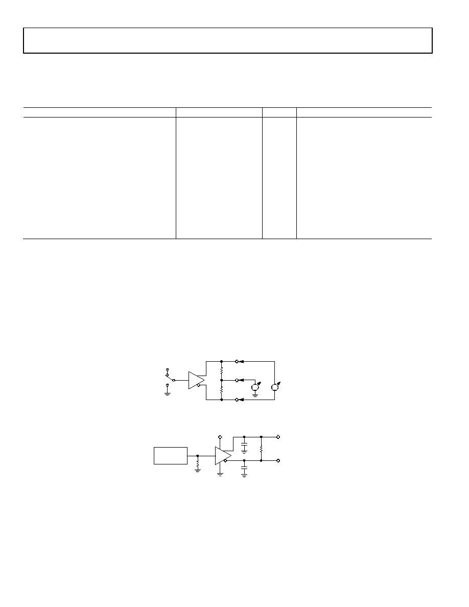
Test Circuits and Timing Diagrams
Figure 2. Test Circuit for Driver VOD and VOS
Figure 3. Test Circuit for Driver Propagation Delay and Transition Time
07032-
002
RL/2
DIN
DOUT+
DOUT–
VCC
VOS
VOD
DRIVER IS ENABLED
V
07032-
003
CL
DIN
DOUT+
DOUT–
DRIVER IS
ENABLED
NOTES
1. CL INCLUDES LOAD AND TEST JIG CAPACITANCE.
SIGNAL
GENERATOR
VCC
50
相关PDF资料 |
PDF描述 |
|---|---|
| ADN4668ARZ-REEL7 | IC RCVR LVDS DIFF 4CH 16SOIC |
| ADN4690EBRZ | IC INTERFACE TXRX |
| ADN4693EBRZ-RL7 | IC TXRX MLVDS 200MBPS 14SOIC |
| ADN4695EBRZ-RL7 | IC TXRX MLVDS 100MBPS 14SOIC |
| ADN4697EBRZ | IC RCVR LVDS 2CH 14SOIC |
相关代理商/技术参数 |
参数描述 |
|---|---|
| ADN4668 | 制造商:AD 制造商全称:Analog Devices 功能描述:3 V LVDS Quad CMOS Differential Line Receiver |
| ADN4668ARUZ | 功能描述:IC RCVR LVDS DIFF 4CH 16TSSOP RoHS:是 类别:集成电路 (IC) >> 接口 - 驱动器,接收器,收发器 系列:- 产品培训模块:RS-232 & USB Transceiver 标准包装:2,000 系列:- 类型:收发器 驱动器/接收器数:1/1 规程:RS232 电源电压:3 V ~ 5.5 V 安装类型:表面贴装 封装/外壳:16-SSOP(0.209",5.30mm 宽) 供应商设备封装:16-SSOP 包装:带卷 (TR) 其它名称:296-19849-2 |
| ADN4668ARUZ1 | 制造商:AD 制造商全称:Analog Devices 功能描述:3 V LVDS Quad CMOS Differential Line Receiver |
| ADN4668ARUZ-REEL7 | 功能描述:IC RCVR LVDS DIFF 4CH 16TSSOP RoHS:是 类别:集成电路 (IC) >> 接口 - 驱动器,接收器,收发器 系列:- 标准包装:121 系列:- 类型:收发器 驱动器/接收器数:1/1 规程:RS422,RS485 电源电压:3 V ~ 3.6 V 安装类型:表面贴装 封装/外壳:10-WFDFN 裸露焊盘 供应商设备封装:10-DFN(3x3) 包装:管件 |
| ADN4668ARUZ-REEL71 | 制造商:AD 制造商全称:Analog Devices 功能描述:3 V LVDS Quad CMOS Differential Line Receiver |
发布紧急采购,3分钟左右您将得到回复。