参数资料
| 型号: | ADN4670BSTZ |
| 厂商: | Analog Devices Inc |
| 文件页数: | 10/12页 |
| 文件大小: | 0K |
| 描述: | IC CLOCK BUFFER MUX 2:10 32LQFP |
| 标准包装: | 1 |
| 类型: | 扇出缓冲器(分配),多路复用器 |
| 电路数: | 1 |
| 比率 - 输入:输出: | 2:10 |
| 差分 - 输入:输出: | 是/是 |
| 输入: | LVDS |
| 输出: | LVDS |
| 频率 - 最大: | 1.1GHz |
| 电源电压: | 2.375 V ~ 2.625 V |
| 工作温度: | -40°C ~ 85°C |
| 安装类型: | 表面贴装 |
| 封装/外壳: | 32-LQFP |
| 供应商设备封装: | 32-LQFP(7x7) |
| 包装: | 托盘 |
Data Sheet
ADN4670
Rev. A | Page 7 of 12
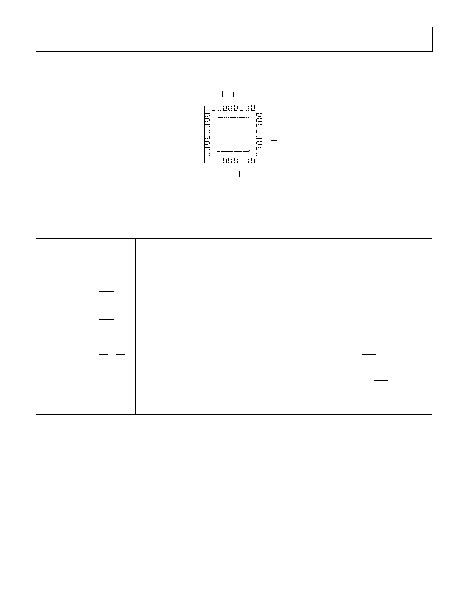
PIN CONFIGURATION AND FUNCTION DESCRIPTIONS
1Q3
2
Q3
3
Q4
4
Q4
5
Q5
6
Q5
7
Q6
8Q6
24
23
22
21
20
19
18
17
CK
SI
CLK0
VBB
CLK1
NOTES
1. THE EXPOSED PAD CAN BE CONNECTED
TO GROUND OR LEFT FLOATING.
EN
9
10
11
12
13
14
15
16
V
SS
Q9
Q8
Q7
V
DD
32
31
30
29
28
27
26
25
V
DD
Q0
Q1
Q2
V
SS
TOP VIEW
(Not to Scale)
ADN4670
088
70
-00
4
Figure 4. Pin Configuration
Table 4. Pin Function Descriptions
Pin No.
Mnemonic
Description
1
CK
Programming Clock. Programming data is clocked in on a low-to-high transition at this input. If left
open-circuit, it is pulled high by a 120 kΩ resistor.
2
SI
Serial Data Input. This is the input for programming data. If left open-circuit, it is pulled low by a 120 kΩ
resistor.
3
CLK0
Noninverting Differential Clock Input 0.
4
CLK0
Inverting Differential Clock Input 0.
5
VBB
Reference Voltage Output.
6
CLK1
Noninverting Differential Clock Input 1.
7
CLK1
Inverting Differential Clock Input 1.
8
EN
Active-High Enable Input. When this input is high, programming is enabled. If left open-circuit, it is
pulled low by a 120 kΩ resistor.
9, 25
VSS
Device Ground.
10, 12, 14, 17, 19,
21, 23, 26, 28, 30
Q9 to Q0
Inverted Clock Output. When the differential input voltage is between CLKx and CLKx > 100 mV, this
output sinks current. When the differential input voltage is between CLKx and CLKx < 100 mV, this
output sources current.
11, 13, 15, 18, 20,
22, 24, 27, 29, 31
Q9 to Q0
Noninverted Clock Output. When the differential input voltage is between CLKx and CLKx > 100 mV,
this output sources current. When the differential input voltage is between CLKx and CLKx < 100 mV,
this output sinks current.
16, 32
VDD
Power Supply Input. This part can be operated from 2.375 V to 2.625 V.
相关PDF资料 |
PDF描述 |
|---|---|
| ADS7864YB/250G4 | IC 12BIT 500KHZ 6CH ADC 48-TQFP |
| ADS7883SBDBVR | IC ADC 12-BIT 3MSPS SOT23-6 |
| ADS8361IDBQG4 | IC ADC DUAL 16BIT 500KSPS 24QSOP |
| ADS8364Y/250G4 | IC ADC LP 16BIT 250KSPS 64-TQFP |
| ADS8412IPFBRG4 | IC ADC 16BIT 2MSPS 48-TQFP |
相关代理商/技术参数 |
参数描述 |
|---|---|
| ADN4670BSTZ-REEL7 | 功能描述:IC CLOCK BUFFER MUX 2:10 32LQFP RoHS:是 类别:集成电路 (IC) >> 时钟/计时 - 时钟缓冲器,驱动器 系列:- 标准包装:74 系列:- 类型:扇出缓冲器(分配) 电路数:1 比率 - 输入:输出:1:10 差分 - 输入:输出:是/是 输入:HCSL, LVCMOS, LVDS, LVPECL, LVTTL 输出:HCSL,LVDS 频率 - 最大:400MHz 电源电压:3 V ~ 3.6 V 工作温度:-40°C ~ 85°C 安装类型:表面贴装 封装/外壳:32-VFQFN 裸露焊盘 供应商设备封装:32-QFN(5x5) 包装:管件 |
| ADN4690E | 制造商:AD 制造商全称:Analog Devices 功能描述:3.3 V, 100 Mbps, Half- and Full-Duplex |
| ADN4690EBRZ | 功能描述:IC INTERFACE TXRX RoHS:是 类别:集成电路 (IC) >> 接口 - 驱动器,接收器,收发器 系列:* 标准包装:98 系列:* |
| ADN4690EBRZ-RL7 | 功能描述:IC TXRX MLVDS 100MBPS 8SOIC RoHS:是 类别:集成电路 (IC) >> 接口 - 驱动器,接收器,收发器 系列:* 标准包装:121 系列:- 类型:收发器 驱动器/接收器数:1/1 规程:RS422,RS485 电源电压:3 V ~ 3.6 V 安装类型:表面贴装 封装/外壳:10-WFDFN 裸露焊盘 供应商设备封装:10-DFN(3x3) 包装:管件 |
| ADN4691E | 制造商:AD 制造商全称:Analog Devices 功能描述:3.3 V, 100 Mbps, Half- and Full-Duplex |
发布紧急采购,3分钟左右您将得到回复。