- 您现在的位置:买卖IC网 > PDF目录16950 > ADP124RHZ-REDYKIT (Analog Devices Inc)REDYKIT 2.8/3.3 ADP124 PDF资料下载
参数资料
| 型号: | ADP124RHZ-REDYKIT |
| 厂商: | Analog Devices Inc |
| 文件页数: | 11/20页 |
| 文件大小: | 0K |
| 描述: | REDYKIT 2.8/3.3 ADP124 |
| 标准包装: | 1 |
| 系列: | Redykit™ |
�� ��
��
��Data� Sheet�
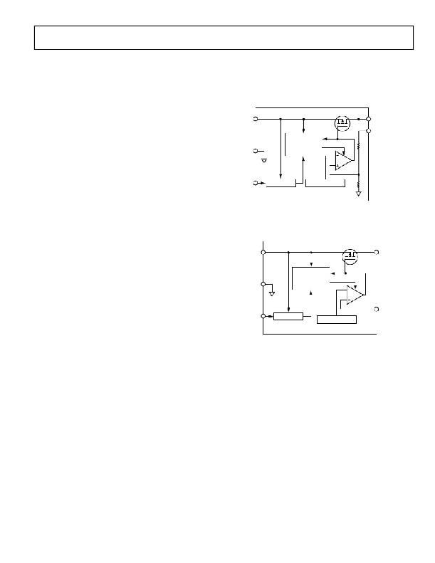
�THEORY� OF� OPERATION�
�The� ADP124/ADP125� are� low� quiescent� current,� low� dropout�
�linear� regulators� that� operate� from� 2.3� V� to� 5.5� V� and� can� provide�
�up� to� 500� mA� of� output� current.� Drawing� a� low� 210� μA� of� quies-�
�cent� current� (typical)� at� full� load� makes� the� ADP124/ADP125�
�ADP124/ADP125�
�The� ADP124/ADP125� use� the� EN� pin� to� enable� and� disable� the�
�VOUT� pin� under� normal� operating� conditions.� When� EN� is� high,�
�VOUT� turns� on;� when� EN� is� low,� VOUT� turns� off.� For� automatic�
�startup,� EN� can� be� tied� to� VIN.�
�ideal� for� battery-operated� portable� equipment.� Shutdown� current�
�consumption� is� typically� 100� nA.�
�Optimized� for� use� with� small� 1� μF� ceramic� capacitors,� the�
�ADP124/ADP125� provide� excellent� transient� performance.�
�Internally,� the� ADP124/ADP125� consist� of� a� reference,� an� error�
�amplifier,� a� feedback� voltage� divider,� and� a� PMOS� pass� transistor.�
�VIN�
�GND�
�ADP124�
�SHORT� CIRCUIT,�
�UVLO,� AND�
�THERMAL�
�PROTECT�
�R1�
�VOUT�
�VOUT� SENSE�
�Output� current� is� delivered� via� the� PMOS� pass� device,� which� is�
�controlled� by� the� error� amplifier.� The� error� amplifier� compares�
�the� reference� voltage� with� the� feedback� voltage� from� the� output�
�EN�
�SHUTDOWN�
�0.5V� REFERENCE�
�R2�
�and� amplifies� the� difference.� If� the� feedback� voltage� is� lower� than�
�the� reference� voltage,� the� gate� of� the� PMOS� device� is� pulled� lower,�
�allowing� more� current� to� pass� and� increasing� the� output� voltage.�
�If� the� feedback� voltage� is� higher� than� the� reference� voltage,� the�
�gate� of� the� PMOS� device� is� pulled� higher,� allowing� less� current�
�to� pass� and� decreasing� the� output� voltage.�
�NOTES�
�1.� R1� AND� R2� ARE� INTERNAL� RESISTORS,� AVAILABLE� ON�
�THE� ADP124� ONLY.�
�Figure� 28.� ADP124� Internal� Block� Diagram� (Fixed� Output)�
�The� adjustable� ADP125� has� an� output� voltage� range� of� 0.8� V� to�
�5.0� V.� The� output� voltage� is� set� by� the� ratio� of� two� external� resistors,�
�VIN�
�ADP125�
�VOUT�
�as� shown� in� Figure� 2.� The� device� servos� the� output� to� maintain�
�the� voltage� at� the� ADJ� pin� at� 0.5� V� referenced� to� ground.� The�
�current� in� R1� is� then� equal� to� 0.5� V/R2� and� the� current� in� R1� is�
�the� current� in� R2� plus� the� ADJ� pin� bias� current.� The� ADJ� pin�
�bias� current,� 15� nA� at� 25°C,� flows� through� R1� into� the� ADJ� pin.�
�GND�
�SHORT� CIRCUIT,�
�UVLO,� AND�
�THERMAL�
�PROTECT�
�The� output� voltage� can� be� calculated� using� the� equation:�
�V� OUT� =� 0.5� V(1� +� R1� /� R2� )� +� (� ADJ� I-BIAS� )(� R1� )�
�EN�
�SHUTDOWN�
�0.5V� REFERENCE�
�ADJ�
�The� value� of� R1� should� be� less� than� 200� k� to� minimize� errors�
�in� the� output� voltage� caused� by� the� ADJ� pin� bias� current.� For�
�example,� when� R1� and� R2� each� equal� 200� kΩ,� the� output� voltage�
�is� 1.0� V.� The� output� voltage� error� introduced� by� the� ADJ� pin�
�bias� current� is� 3� mV� or� 0.3%,� assuming� a� typical� ADJ� pin� bias�
�current� of� 15� nA� at� 25°C.�
�Note� that� in� shutdown,� the� output� is� turned� off� and� the� divider�
�current� is� 0.�
�Rev.� C� |� Page� 11� of� 20�
�Figure� 29.� ADP125� Internal� Block� Diagram� (Adjustable� Output)�
�相关PDF资料 |
PDF描述 |
|---|---|
| ESM12DSEI-S243 | CONN EDGECARD 24POS .156 EYELET |
| ADP150UJZ-REDYKIT | KIT REDI TOOL 1.8/3.3 ADP150 |
| VI-J5P-EY | CONVERTER MOD DC/DC 13.8V 50W |
| ESM08DTKT-S288 | CONN EDGECARD 16POS .156 EXTEND |
| ESM08DTBN-S189 | CONN EDGECARD 16POS R/A .156 SLD |
相关代理商/技术参数 |
参数描述 |
|---|---|
| ADP125 | 制造商:AD 制造商全称:Analog Devices 功能描述:5.5 V Input, 500 mA, Low Quiescent Current, CMOS Linear Regulators |
| ADP1250001RHZR | 制造商:Analog Devices 功能描述: |
| ADP1251 | 制造商:未知厂家 制造商全称:未知厂家 功能描述:PRECISION SEMICONDUCTOR PRESSURE SENSOR |
| ADP125ACPZ-R7 | 功能描述:IC REG LDO ADJ .5A 8LFCSP RoHS:是 类别:集成电路 (IC) >> PMIC - 稳压器 - 线性 系列:- 标准包装:45 系列:- 稳压器拓扑结构:正,固定式 输出电压:5V 输入电压:6 V ~ 30 V 电压 - 压降(标准):0.47V @ 250mA 稳压器数量:1 电流 - 输出:250mA 电流 - 限制(最小):- 工作温度:-40°C ~ 125°C 安装类型:通孔 封装/外壳:TO-220-3 供应商设备封装:TO-220-3 包装:管件 产品目录页面:1289 (CN2011-ZH PDF) 其它名称:*LP2954AIT*LP2954AIT/NOPBLP2954AIT |
| ADP125ARHZ | 功能描述:IC REG LDO ADJ .5A 8MSOP RoHS:是 类别:集成电路 (IC) >> PMIC - 稳压器 - 线性 系列:- 标准包装:3,000 系列:- 稳压器拓扑结构:正,固定式 输出电压:3V 输入电压:最高 5.5V 电压 - 压降(标准):0.12V @ 150mA 稳压器数量:1 电流 - 输出:150mA(最小值) 电流 - 限制(最小):220mA 工作温度:-40°C ~ 125°C 安装类型:表面贴装 封装/外壳:SOT-23-5 细型,TSOT-23-5 供应商设备封装:TSOT-23-5 包装:带卷 (TR) 其它名称:ADP160AUJZ-3.0-R7TR |
发布紧急采购,3分钟左右您将得到回复。