- 您现在的位置:买卖IC网 > PDF目录16976 > ADP125-EVALZ (Analog Devices Inc)BOARD EVALUATION ADJUSTABLE V PDF资料下载
参数资料
| 型号: | ADP125-EVALZ |
| 厂商: | Analog Devices Inc |
| 文件页数: | 13/20页 |
| 文件大小: | 0K |
| 描述: | BOARD EVALUATION ADJUSTABLE V |
| 标准包装: | 1 |
| 每 IC 通道数: | 1 - 单 |
| 输出电压: | 0.8 ~ 5 V |
| 电流 - 输出: | 500mA |
| 输入电压: | 2.3 ~ 5.5 V |
| 稳压器类型: | 正,可调式 |
| 工作温度: | -40°C ~ 85°C |
| 板类型: | 完全填充 |
| 已供物品: | 板 |
| 已用 IC / 零件: | ADP125 |
�� �
�
�Data� Sheet�
�In� this� example,� the� worst-case� temperature� coefficient� (TEMPCO)�
�over� ?40°C� to� +85°C� is� assumed� to� be� 15%� for� an� X5R� dielectric.�
�The� tolerance� of� the� capacitor� (TOL)� is� assumed� to� be� 10%,� and�
��Substituting� these� values� in� Equation� 1� yields�
�C� EFF� =� 0.94� μF� ×� (1� ?� 0.15)� ×� (1� ?� 0.1)� =� 0.719� μF�
�Therefore,� the� capacitor� chosen� in� this� example� meets� the�
�ADP124/ADP125�
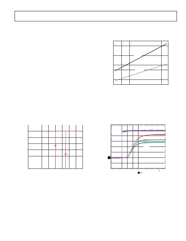
�The� active� and� inactive� thresholds� of� the� EN� pin� are� derived� from�
�the� VIN� voltage.� Therefore,� these� thresholds� vary� as� the� input�
�voltage� changes.� Figure� 34� shows� typical� EN� active� and� inactive�
�thresholds� when� the� VIN� voltage� varies� from� 2.3� V� to� 5.5� V.�
�1.05�
�1.00�
�0.95�
�minimum� capacitance� requirement� of� the� LDO� over� tem-�
�perature� and� tolerance� at� the� chosen� output� voltage.�
�To� guarantee� the� performance� of� the� ADP124/ADP125,� it� is�
�imperative� that� the� effects� of� dc� bias,� temperature,� and� tolerances�
�on� the� behavior� of� the� capacitors� are� evaluated� for� each� application.�
�0.90�
�0.85�
�0.80�
�0.75�
�RISING�
�FALLING�
�UNDERVOLTAGE� LOCKOUT�
�The� ADP124/ADP125� have� an� internal� undervoltage� lockout�
�circuit� that� disables� all� inputs� and� the� output� when� the� input�
�voltage� is� less� than� approximately� 2� V.� This� ensures� that� the�
�ADP124/ADP125� inputs� and� the� output� behave� in� a� predictable�
�manner� during� power-up.�
�ENABLE� FEATURE�
�The� ADP124/ADP125� uses� the� EN� pin� to� enable� and� disable� the�
�VOUT� pin� under� normal� operating� conditions.� As� shown� in�
��VOUT� turns� on.� Conversely,� when� a� falling� voltage� on� EN� crosses�
�the� inactive� threshold,� VOUT� turns� off.�
�0.70�
�0.65�
�0.60�
�2.2� 2.7� 3.2� 3.7� 4.2� 4.7� 5.2�
�V� IN� (V)�
�Figure� 34.� Typical� EN� Pin� Thresholds� vs.� Input� Voltage�
�The� ADP124/ADP125� use� an� internal� soft� start� to� limit� the�
�inrush� current� when� the� output� is� enabled.� The� start-up� time�
�for� the� 2.8� V� option� is� approximately� 350� μs� from� the� time� the�
�EN� active� threshold� is� crossed� to� when� the� output� reaches� 90%�
�of� its� final� value.� As� shown� in� Figure� 35,� the� start-up� time� is�
�dependent� on� the� output� voltage� setting� and� increases� slightly�
�as� the� output� voltage� increases.�
�3.5�
�V� IN� =� 5V�
�3.0�
�V� OUT� =� 4.2V�
�2.5�
�2.0�
�1.5�
�1.0�
�0.5�
�0�
�1�
�2�
�V� OUT� =� 3.3V�
�V� OUT� =� 2.8V�
�0�
�0.2�
�0.4�
�0.6�
�0.8�
�1.0�
�1.2�
�1.4�
�1.6�
�CH1� 1.00V�
�CH2� 1.00V�
�B�
�W�
�M100μs�
�A� CH1�
�2.00V�
�V� EN�
�T�
�296.800μs�
�Figure� 33.� Typical� EN� Pin� Operation�
�As� shown� in� Figure� 33,� the� EN� pin� has� built-in� hysteresis.� This�
�prevents� on/off� oscillations� that� may� occur� due� to� noise� on� the�
�EN� pin� as� it� passes� through� the� threshold� points.�
�Rev.� C� |� Page� 13� of� 20�
�Figure� 35.� Typical� Start-Up� Time�
�相关PDF资料 |
PDF描述 |
|---|---|
| ECC35DJXN-S1136 | CONN EDGECARD 70PS .100 PRESSFIT |
| HBM12DRXI | CONN EDGECARD 24POS DIP .156 SLD |
| MIC94310-GYMT EV | BOARD EVAL FOR MIC94310-GYMT |
| LM285Z/NOPB | IC VREF SHUNT ADJ TO-92-3 |
| 3-1589472-6 | CONN PLUG 15POS 30AWG 10IN |
相关代理商/技术参数 |
参数描述 |
|---|---|
| ADP1261 | 制造商:未知厂家 制造商全称:未知厂家 功能描述:PRECISION SEMICONDUCTOR PRESSURE SENSOR |
| ADP1271 | 功能描述:板上安装压力/力传感器 490.3kPa 5.0kgf/cm Pressure Sensor RoHS:否 制造商:Honeywell 工作压力:0 bar to 4 bar 压力类型:Gage 准确性:+ / - 0.25 % 输出类型:Digital 安装风格:Through Hole 工作电源电压:5 V 封装 / 箱体:SIP 端口类型:Dual Radial Barbed, Same sides |
| ADP1281 | 制造商:未知厂家 制造商全称:未知厂家 功能描述:PRECISION SEMICONDUCTOR PRESSURE SENSOR |
| ADP1290ACBZ-R7 | 功能描述:IC LOAD SWITCH HIGH SIDE 6WLCSP 制造商:analog devices inc. 系列:- 包装:剪切带(CT) 零件状态:有效 开关类型:通用 输出数:1 比率 - 输入:输出:1:1 输出配置:高端 输出类型:N 通道 接口:开/关 电压 - 负载:2.3 V ~ 13.2 V 电压 - 电源(Vcc/Vdd):不需要 电流 - 输出(最大值):2A 导通电阻(典型值):40 毫欧 输入类型:- 特性:- 故障保护:- 工作温度:-40°C ~ 105°C(TJ) 封装/外壳:6-WFBGA,WLCSP 供应商器件封装:6-WLCSP(1.45x0.95) 标准包装:1 |
| ADP1290CB-EVALZ | 功能描述:ADP1290 - Power Management, Power Distribution Switch (Load Switch) Evaluation Board 制造商:analog devices inc. 系列:- 零件状态:有效 主要用途:电源管理,配电开关(负载开关) 嵌入式:- 使用的 IC/零件:ADP1290 主要属性:1 通道(单路) 辅助属性:- 所含物品:板 标准包装:1 |
发布紧急采购,3分钟左右您将得到回复。