- 您现在的位置:买卖IC网 > PDF目录4814 > ADP160ACBZ-1.5-R7 (Analog Devices Inc)IC REG LDO 1.5V .15A 4WLCSP PDF资料下载
参数资料
| 型号: | ADP160ACBZ-1.5-R7 |
| 厂商: | Analog Devices Inc |
| 文件页数: | 16/24页 |
| 文件大小: | 0K |
| 描述: | IC REG LDO 1.5V .15A 4WLCSP |
| 产品变化通告: | 8mm Carrier Tape Changes 28/Feb/2012 |
| 标准包装: | 3,000 |
| 稳压器拓扑结构: | 正,固定式 |
| 输出电压: | 1.5V |
| 输入电压: | 2.2 V ~ 5.5 V |
| 稳压器数量: | 1 |
| 电流 - 输出: | 150mA(最小值) |
| 电流 - 限制(最小): | 220mA |
| 工作温度: | -40°C ~ 125°C |
| 安装类型: | 表面贴装 |
| 封装/外壳: | 4-UFBGA,WLCSP |
| 供应商设备封装: | 4-WLCSP(0.96x0.96) |
| 包装: | 带卷 (TR) |
�� �
�
�ADP160/ADP161/ADP162/ADP163�
�Consider� the� case� where� a� hard� short� from� OUT� to� ground�
�occurs.� At� first,� the� ADP16x� current� limit� so� that� only� 320� mA�
�Table� 9.� Typical� Ψ� JB� Values�
�Ψ� JB� (°C/W)�
�Data� Sheet�
�is� conducted� into� the� short.� If� self-heating� of� the� junction� is�
�great� enough� to� cause� its� temperature� to� rise� above� 150°C,�
�thermal� shutdown� activates,� turning� off� the� output� and�
�reducing� the� output� current� to� zero.� As� the� junction� tempera-�
�ture� cools� and� drops� below� 135°C,� the� output� turns� on� and�
�conducts� 320� mA� into� the� short,� again� causing� the� junction�
�TSOT� WLCSP�
�42.8� 58.4�
�The� junction� temperature� of� the� ADP16x� can� be� calculated�
�from� the� following� equation:�
�T� J� =� T� A� +� (� P� D� ×� θ� JA� )�
�(2)�
�temperature� to� rise� above� 150°C.� This� thermal� oscillation�
�between� 135°C� and� 150°C� causes� a� current� oscillation� between�
�320� mA� and� 0� mA� that� continues� as� long� as� the� short� remains�
�at� the� output.�
�Current� and� thermal� limit� protections� are� intended� to� protect�
�the� device� against� accidental� overload� conditions.� For� reliable�
�operation,� device� power� dissipation� must� be� externally� limited�
�so� junction� temperatures� do� not� exceed� 125°C.�
�THERMAL� CONSIDERATIONS�
�In� most� applications,� the� ADP16x� do� not� dissipate� much� heat� due�
�to� their� high� efficiency.� However,� in� applications� with� high� ambient�
�temperature� and� high� supply� voltage� to� output� voltage� differential,�
�the� heat� dissipated� in� the� package� is� large� enough� that� it� can� cause�
�the� junction� temperature� of� the� die� to� exceed� the� maximum�
�junction� temperature� of� 125°C.�
�When� the� junction� temperature� exceeds� 150°C,� the� converter� enters�
�thermal� shutdown.� It� recovers� only� after� the� junction� temperature�
�has� decreased� below� 135°C� to� prevent� any� permanent� damage.�
�Therefore,� thermal� analysis� for� the� chosen� application� is� very�
�important� to� guarantee� reliable� performance� over� all� conditions.�
�The� junction� temperature� of� the� die� is� the� sum� of� the� ambient�
�temperature� of� the� environment� and� the� temperature� rise� of� the�
�package� due� to� the� power� dissipation,� as� shown� in� Equation� 2.�
�To� guarantee� reliable� operation,� the� junction� temperature� of�
�the� ADP16x� must� not� exceed� 125°C.� To� ensure� the� junction�
�temperature� stays� below� this� maximum� value,� the� user� needs� to�
�be� aware� of� the� parameters� that� contribute� to� junction� temperature�
�changes.� These� parameters� include� ambient� temperature,� power�
�dissipation� in� the� power� device,� and� thermal� resistances� between�
�the� junction� and� ambient� air� (θ� JA� ).� The� θ� JA� number� is� dependent�
�on� the� package� assembly� compounds� that� are� used� and� the� amount�
�of� copper� used� to� solder� the� package� GND� pins� to� the� PCB.�
��4-ball� WLCSP� for� various� PCB� copper� sizes.� Table� 9� shows� the�
�typical� Ψ� JB� value� of� the� 5-lead� TSOT� and� 4-ball� WLCSP.�
�Table� 8.� Typical� θ� JA� Values�
�θ� JA� (°C/W)�
�where:�
�T� A� is� the� ambient� temperature.�
�P� D� is� the� power� dissipation� in� the� die,� given� by�
�P� D� =� [(� V� IN� ?� V� OUT� )� � I� LOAD� ]� +� (� V� IN� � I� GND� )� (3)�
�where:�
�I� LOAD� is� the� load� current.�
�I� GND� is� the� ground� current.�
�V� IN� and� V� OUT� are� input� and� output� voltages,� respectively.�
�Power� dissipation� due� to� ground� current� is� quite� small� and� can� be�
�ignored.� Therefore,� the� junction� temperature� equation� simplifies� to�
�the� following:�
�T� J� =� T� A� +� {[(� V� IN� ?� V� OUT� )� ×� I� LOAD� ]� ×� θ� JA� }� (4)�
�As� shown� in� Equation� 4,� for� a� given� ambient� temperature,� input-�
�to-output� voltage� differential,� and� continuous� load� current,� there�
�exists� a� minimum� copper� size� requirement� for� the� PCB� to� ensure�
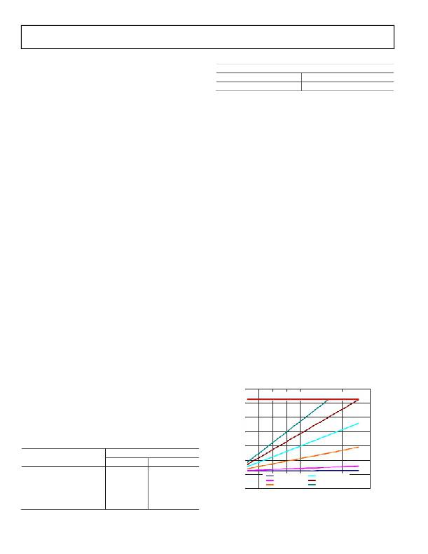
�the� junction� temperature� does� not� rise� above� 125°C.� Figure� 41� to�
��different� ambient� temperatures,� load� currents,� V� IN� -to-V� OUT�
�differentials,� and� areas� of� PCB� copper.�
�In� the� case� where� the� board� temperature� is� known,� use� the�
�thermal� characterization� parameter,� Ψ� JB� ,� to� estimate� the� junction�
�temperature� rise� (see� Figure� 49� and� Figure� 50).� Maximum�
�junction� temperature� (T� J� )� is� calculated� from� the� board�
�temperature� (T� B� )� and� power� dissipation� (P� D� )� using� the�
�following� formula:�
�T� J� =� T� B� +� (� P� D� ×� Ψ� JB� )� (5)�
�The� typical� value� of� Ψ� JB� is� 58°C/W� for� the� 4-ball� WLCSP� package�
�and� 43°C/W� for� the� 5-lead� TSOT� package.�
�140�
�MAXIMUM� JUNCTION� TEMPERATURE�
�120�
�100�
�80�
�60�
�Copper� Size� (mm� 2� )�
�TSOT�
�WLCSP�
�40�
�I� LOAD� =� 1mA�
�I� LOAD� =� 100mA�
�0� 1�
�50�
�100�
�300�
�500�
�170�
�152�
�146�
�134�
�131�
�260�
�159�
�157�
�153�
�151�
�20�
�I� LOAD� =� 10mA� I� LOAD� =� 150mA�
�I� LOAD� =� 50mA� I� LOAD� =� 200mA�
�0�
�0.3� 0.8� 1.3� 1.8� 2.3� 2.8� 3.3� 3.8� 4.3�
�V� IN� –� V� OUT� (V)�
�Figure� 41.� 500� mm� 2� of� PCB� Copper,� WLCSP,� T� A� =� 25°C�
�4.8�
�1�
�Device� soldered� to� minimum� size� pin� traces.�
�Rev.� H� |� Page� 16� of� 24�
�相关PDF资料 |
PDF描述 |
|---|---|
| AMC12DRYN | CONN EDGECARD 24POS .100 DIP SLD |
| AMC12DRYH | CONN EDGECARD 24POS .100 DIP SLD |
| ADP160ACBZ-1.2-R7 | IC REG LDO 1.2V .15A 4WLCSP |
| ADP151ACBZ-2.8-R7 | IC REG LDO 2.8V .2A 4WLCSP |
| MC7815ACD2TG | IC REG LDO 15V 1A D2PAK |
相关代理商/技术参数 |
参数描述 |
|---|---|
| ADP160ACBZ-2.1-R7 | 功能描述:IC REG LDO 2.1V .15A 4WLCSP RoHS:是 类别:集成电路 (IC) >> PMIC - 稳压器 - 线性 系列:- 其它有关文件:LD39015JXX12 View All Specifications 标准包装:1 系列:- 稳压器拓扑结构:正,固定式 输出电压:1.2V 输入电压:1.5 V ~ 5.5 V 电压 - 压降(标准):- 稳压器数量:1 电流 - 输出:150mA 电流 - 限制(最小):- 工作温度:-40°C ~ 125°C 安装类型:表面贴装 封装/外壳:4-WFBGA,FCBGA 供应商设备封装:4-覆晶(1.07x1.07) 包装:Digi-Reel® 其它名称:497-11958-6 |
| ADP160ACBZ-2.3-R7 | 制造商:AD 制造商全称:Analog Devices 功能描述:Ultralow Quiescent Current, 150 mA, CMOS Linear Regulators |
| ADP160ACBZ-2.5-R7 | 功能描述:IC REG LDO 2.5V .15A 4WLCSP RoHS:是 类别:集成电路 (IC) >> PMIC - 稳压器 - 线性 系列:- 其它有关文件:LD39015JXX12 View All Specifications 标准包装:1 系列:- 稳压器拓扑结构:正,固定式 输出电压:1.2V 输入电压:1.5 V ~ 5.5 V 电压 - 压降(标准):- 稳压器数量:1 电流 - 输出:150mA 电流 - 限制(最小):- 工作温度:-40°C ~ 125°C 安装类型:表面贴装 封装/外壳:4-WFBGA,FCBGA 供应商设备封装:4-覆晶(1.07x1.07) 包装:Digi-Reel® 其它名称:497-11958-6 |
| ADP160ACBZ-2.75-R7 | 功能描述:IC REG LDO 2.75V .15A 4WLCSP RoHS:是 类别:集成电路 (IC) >> PMIC - 稳压器 - 线性 系列:- 其它有关文件:LD39015JXX12 View All Specifications 标准包装:1 系列:- 稳压器拓扑结构:正,固定式 输出电压:1.2V 输入电压:1.5 V ~ 5.5 V 电压 - 压降(标准):- 稳压器数量:1 电流 - 输出:150mA 电流 - 限制(最小):- 工作温度:-40°C ~ 125°C 安装类型:表面贴装 封装/外壳:4-WFBGA,FCBGA 供应商设备封装:4-覆晶(1.07x1.07) 包装:Digi-Reel® 其它名称:497-11958-6 |
| ADP160ACBZ-2.7-R7 | 制造商:AD 制造商全称:Analog Devices 功能描述:Ultralow Quiescent Current, 150 mA, CMOS Linear Regulators |
发布紧急采购,3分钟左右您将得到回复。