- 您现在的位置:买卖IC网 > PDF目录20391 > ADP1612-5-EVALZ (Analog Devices Inc)BOARD EVAL ADP1612 5V VOUT PDF资料下载
参数资料
| 型号: | ADP1612-5-EVALZ |
| 厂商: | Analog Devices Inc |
| 文件页数: | 24/28页 |
| 文件大小: | 0K |
| 描述: | BOARD EVAL ADP1612 5V VOUT |
| 标准包装: | 1 |
| 主要目的: | DC/DC,步升 |
| 输出及类型: | 1,非隔离 |
| 输出电压: | 5V |
| 电流 - 输出: | 1.4A |
| 输入电压: | 1.8 ~ 5.5 V |
| 稳压器拓扑结构: | 升压 |
| 板类型: | 完全填充 |
| 已供物品: | 板 |
| 已用 IC / 零件: | ADP1612 |
| 产品目录页面: | 791 (CN2011-ZH PDF) |
| 相关产品: | ADP1612ARMZ-R7DKR-ND - IC REG BST SEPIC ADJ 1.4A 8MSOP ADP1612ARMZ-R7CT-ND - IC REG BST SEPIC ADJ 1.4A 8MSOP ADP1612ARMZ-R7TR-ND - IC REG BST SEPIC ADJ 1.4A 8MSOP |
第1页第2页第3页第4页第5页第6页第7页第8页第9页第10页第11页第12页第13页第14页第15页第16页第17页第18页第19页第20页第21页第22页第23页当前第24页第25页第26页第27页第28页
�� ��
��
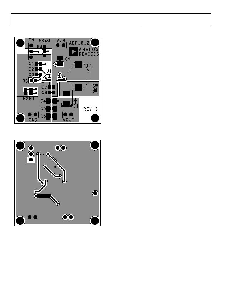
��ADP1612/ADP1613�
�Data� Sheet�
�PCB� LAYOUT� GUIDELINES�
�For� high� efficiency,� good� regulation,� and� stability,� a� well-designed�
�printed� circuit� board� layout� is� required.�
�Use� the� following� guidelines� when� designing� printed� circuit�
��for� a� pin� configuration).�
�?�
�?�
�?�
�?�
�?�
�Keep� the� low� ESR� input� capacitor,� C� IN� (labeled� as� C7� in�
��injected� into� the� part� from� board� parasitic� inductance.�
�Keep� the� high� current� path� from� C� IN� (labeled� as� C7� in�
��short� as� possible.�
�Keep� the� high� current� path� from� VIN� through� L1,� the�
�rectifier� (D1)� and� the� output� capacitor,� C� OUT� (labeled� as�
�C4� in� Figure� 76)� as� short� as� possible.�
�Keep� high� current� traces� as� short� and� as� wide� as� possible.�
�Place� the� feedback� resistors� as� close� to� FB� as� possible� to�
�prevent� noise� pickup.� Connect� the� ground� of� the� feedback�
�network� directly� to� an� AGND� plane� that� makes� a� Kelvin�
�Figure� 76.� Example� Layout� for� ADP1612/ADP1613� Boost� Application�
�(Top� Layer)�
�?�
�?�
�?�
�connection� to� the� GND� pin.�
�Place� the� compensation� components� as� close� as� possible� to�
�COMP.� Connect� the� ground� of� the� compensation� network�
�directly� to� an� AGND� plane� that� makes� a� Kelvin� connection�
�to� the� GND� pin.�
�Connect� the� softstart� capacitor,� C� SS� (labeled� as� C1� in�
��ground� of� the� softstart� capacitor� to� an� AGND� plane� that�
�makes� a� Kelvin� connection� to� the� GND� pin.�
�Avoid� routing� high� impedance� traces� from� the� compensa-�
�tion� and� feedback� resistors� near� any� node� connected� to� SW�
�or� near� the� inductor� to� prevent� radiated� noise� injection.�
�Figure� 77.� Example� Layout� for� ADP1612/ADP1613� Boost� Application�
�(Bottom� Layer)�
�Rev.� D� |� Page� 24� of� 28�
�相关PDF资料 |
PDF描述 |
|---|---|
| R0.25D12-3.315/H-R | CONV DC/DC 0.25W 3.3V +/-15VOUT |
| SDR1005-470KL | INDUCTOR 47UH SMD POWER |
| MLK0603L3N9S | INDUCTOR 3.9NH +-.3NH FIXED 0201 |
| T95C107M016LSSL | CAP TANT 100UF 16V 20% 2812 |
| VI-B3D-CX-F4 | CONVERTER MOD DC/DC 85V 75W |
相关代理商/技术参数 |
参数描述 |
|---|---|
| ADP1612ARMZ-R7 | 功能描述:IC REG BST SEPIC ADJ 1.4A 8MSOP RoHS:是 类别:集成电路 (IC) >> PMIC - 稳压器 - DC DC 开关稳压器 系列:- 产品培训模块:High Efficiency Current Mode Switching Regulators CMOS LDO Regulators 特色产品:BD91x Series Step-Down Regulators 标准包装:2,500 系列:- 类型:降压(降压) 输出类型:两者兼有 输出数:2 输出电压:3.3V,0.8 V ~ 2.5 V 输入电压:4.5 V ~ 5.5 V PWM 型:电流模式 频率 - 开关:1MHz 电流 - 输出:1.5A 同步整流器:是 工作温度:-40°C ~ 85°C 安装类型:表面贴装 封装/外壳:20-VFQFN 裸露焊盘 包装:带卷 (TR) 供应商设备封装:VQFN020V4040 产品目录页面:1373 (CN2011-ZH PDF) 其它名称:BD9152MUV-E2TR |
| ADP1612-BL1-EVZ | 制造商:Analog Devices 功能描述:BLANK ADISIMPOWER EVAL ADP1612 - Boxed Product (Development Kits) |
| ADP1612-BL2-EVZ | 制造商:Analog Devices 功能描述:BLANK SEPIC DEMO BOARD - Boxed Product (Development Kits) |
| ADP1612-BL3-EVZ | 功能描述:EVAL BLANK ADISIMPOWER ADP1612 RoHS:是 类别:编程器,开发系统 >> 评估板 - DC/DC 与 AC/DC(离线)SMPS 系列:- 标准包装:1 系列:- 主要目的:DC/DC,步降 输出及类型:1,非隔离 功率 - 输出:- 输出电压:3.3V 电流 - 输出:3A 输入电压:4.5 V ~ 28 V 稳压器拓扑结构:降压 频率 - 开关:250kHz 板类型:完全填充 已供物品:板 已用 IC / 零件:L7981 其它名称:497-12113STEVAL-ISA094V1-ND |
| ADP1613 | 制造商:AD 制造商全称:Analog Devices 功能描述:650 kHz /1.3 MHz Step-Up PWM DC-to-DC Switching Converters |
发布紧急采购,3分钟左右您将得到回复。