- 您现在的位置:买卖IC网 > PDF目录5195 > ADP1711AUJZ-0.9-R7 (Analog Devices Inc)IC REG LDO 0.9V .15A TSOT-23-5 PDF资料下载
参数资料
| 型号: | ADP1711AUJZ-0.9-R7 |
| 厂商: | Analog Devices Inc |
| 文件页数: | 10/16页 |
| 文件大小: | 0K |
| 描述: | IC REG LDO 0.9V .15A TSOT-23-5 |
| 产品培训模块: | Power Line Monitoring |
| 标准包装: | 1 |
| 稳压器拓扑结构: | 正,固定式 |
| 输出电压: | 0.9V |
| 输入电压: | 2.5 V ~ 5.5 V |
| 稳压器数量: | 1 |
| 电流 - 输出: | 150mA(最小值) |
| 电流 - 限制(最小): | 180mA |
| 工作温度: | -40°C ~ 125°C |
| 安装类型: | 表面贴装 |
| 封装/外壳: | SOT-23-5 细型,TSOT-23-5 |
| 供应商设备封装: | TSOT-23-5 |
| 包装: | 标准包装 |
| 产品目录页面: | 793 (CN2011-ZH PDF) |
| 配用: | ADP1711-2.5-EVALZ-ND - BOARD EVAL FOR ADP1711-2.5 |
| 其它名称: | ADP1711AUJZ-0.9-R7DKR |
�� ��
��
��ADP1710/ADP1711�
�APPLICATION� INFORMATION�
�CAPACITOR� SELECTION�
�Output� Capacitor�
�The� ADP1710/ADP1711� are� designed� for� operation� with� small,�
�space-saving� ceramic� capacitors,� but� they� will� function� with� most�
�commonly� used� capacitors� as� long� as� care� is� taken� about� the�
�effective� series� resistance� (ESR)� value.� The� ESR� of� the� output�
�capacitor� affects� stability� of� the� LDO� control� loop.� A� minimum� of�
�1� μF� capacitance� with� an� ESR� of� 500� mΩ� or� less� is� recommended�
�to� ensure� stability� of� the� ADP1710/ADP1711.� Transient� response�
�to� changes� in� load� current� is� also� affected� by� output� capacitance.�
�Using� a� larger� value� of� output� capacitance� improves� the� transient�
�response� of� the� ADP1710/ADP1711� to� large� changes� in� load�
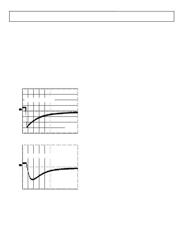
�current.� Figure� 21� and� Figure� 22� show� the� transient� responses� for�
�output� capacitance� values� of� 1� μF� and� 22� μF,� respectively.�
�V� OUT� RESPONSE� TO� LOAD� STEP�
�FROM� 7.5mA� TO� 142.5mA�
�1�
�V� IN� =� 5V�
�V� OUT� =� 3.3V�
�C� IN� =� 1μF�
�C� OUT� =� 1μF�
�TIME� (4μs/DIV)�
�Figure� 21.� Output� Transient� Response,� C� OUT� =� 1� μF�
�V� OUT� RESPONSE� TO� LOAD� STEP�
�FROM� 7.5mA� TO� 142.5mA�
�1�
�V� IN� =� 5V�
�V� OUT� =� 3.3V�
�C� IN� =� 22μF�
�C� OUT� =� 22μF�
�TIME� (4μs/DIV)�
�Figure� 22.� Output� Transient� Response,� C� OUT� =� 22� μF�
�Input� Bypass� Capacitor�
�Connecting� a� 1� μF� capacitor� from� IN� to� GND� reduces� the�
�circuit� sensitivity� to� printed� circuit� board� (PCB)� layout,�
�especially� when� long� input� traces� or� high� source� impedance� are�
�encountered.� If� greater� than� 1� μF� of� output� capacitance� is�
�required,� the� input� capacitor� should� be� increased� to� match� it.�
�Input� and� Output� Capacitor� Properties�
�Any� good� quality� ceramic� capacitors� can� be� used� with� the�
�ADP1710/ADP1711,� as� long� as� they� meet� the� minimum�
�capacitance� and� maximum� ESR� requirements.� Ceramic�
�capacitors� are� manufactured� with� a� variety� of� dielectrics,� each�
�with� different� behavior� over� temperature� and� applied� voltage.�
�Capacitors� must� have� a� dielectric� adequate� to� ensure� the�
�minimum� capacitance� over� the� necessary� temperature� range�
�and� dc� bias� conditions.� X5R� or� X7R� dielectrics� with� a� voltage�
�rating� of� 6.3� V� or� 10� V� are� recommended.� Y5V� and� Z5U�
�dielectrics� are� not� recommended,� due� to� their� poor� temperature�
�and� dc� bias� characteristics.�
�CURRENT� LIMIT� AND� THERMAL� OVERLOAD�
�PROTECTION�
�The� ADP1710/ADP1711� are� protected� against� damage� due� to�
�excessive� power� dissipation� by� current� and� thermal� overload�
�protection� circuits.� The� ADP1710/ADP1711� are� designed� to�
�current� limit� when� the� output� load� reaches� 270� mA� (typical).�
�When� the� output� load� exceeds� 270� mA,� the� output� voltage� is�
�reduced� to� maintain� a� constant� current� limit.�
�Thermal� overload� protection� is� included,� which� limits� the�
�junction� temperature� to� a� maximum� of� 150°C� (typical).� Under�
�extreme� conditions� (that� is,� high� ambient� temperature� and�
�power� dissipation)� when� the� junction� temperature� starts� to� rise�
�above� 150°C,� the� output� is� turned� off,� reducing� the� output�
�current� to� zero.� When� the� junction� temperature� drops� below�
�135°C,� the� output� is� turned� on� again� and� output� current� is�
�restored� to� its� nominal� value.�
�Consider� the� case� where� a� hard� short� from� OUT� to� ground�
�occurs.� At� first� the� ADP1710/ADP1711� current� limits,� so� that�
�only� 270� mA� is� conducted� into� the� short.� If� self� heating� of� the�
�junction� is� great� enough� to� cause� its� temperature� to� rise� above�
�150°C,� thermal� shutdown� activates,� turning� off� the� output� and�
�reducing� the� output� current� to� zero.� As� the� junction�
�temperature� cools� and� drops� below� 135°C,� the� output� turns� on�
�and� conducts� 270� mA� into� the� short,� again� causing� the�
�junction� temperature� to� rise� above� 150°C.� This� thermal�
�oscillation� between� 135°C� and� 150°C� causes� a� current�
�oscillation� between� 270� mA� and� 0� mA,� which� continues� as�
�long� as� the� short� remains� at� the� output.�
�Rev.� 0� |� Page� 10� of� 16�
�相关PDF资料 |
PDF描述 |
|---|---|
| HMC15DREH-S93 | CONN EDGECARD 30POS .100 EYELET |
| GSC17DRTN-S13 | CONN EDGECARD 34POS .100 EXTEND |
| GMC17DRTN-S13 | CONN EDGECARD 34POS .100 EXTEND |
| LT3022IDHC#PBF | IC REG LDO ADJ 1A 16DFN |
| LT3029IDE#PBF | IC REG LDO ADJ .5A 16DFN |
相关代理商/技术参数 |
参数描述 |
|---|---|
| ADP1711AUJZ-1.05R7 | 功能描述:IC REG LDO 1.05V .15A TSOT-23-5 RoHS:是 类别:集成电路 (IC) >> PMIC - 稳压器 - 线性 系列:- 标准包装:3,000 系列:- 稳压器拓扑结构:正,固定式 输出电压:2.5V 输入电压:2.5 V ~ 5.5 V 电压 - 压降(标准):- 稳压器数量:1 电流 - 输出:300mA(最小值) 电流 - 限制(最小):360mA 工作温度:-40°C ~ 85°C 安装类型:表面贴装 封装/外壳:SOT-23-5 细型,TSOT-23-5 供应商设备封装:TSOT-23-5 包装:带卷 (TR) |
| ADP1711AUJZ-1.0-R7 | 功能描述:IC REG LDO 1V .15A TSOT-23-5 RoHS:是 类别:集成电路 (IC) >> PMIC - 稳压器 - 线性 系列:- 标准包装:45 系列:- 稳压器拓扑结构:正,固定式 输出电压:5V 输入电压:6 V ~ 30 V 电压 - 压降(标准):0.47V @ 250mA 稳压器数量:1 电流 - 输出:250mA 电流 - 限制(最小):- 工作温度:-40°C ~ 125°C 安装类型:通孔 封装/外壳:TO-220-3 供应商设备封装:TO-220-3 包装:管件 产品目录页面:1289 (CN2011-ZH PDF) 其它名称:*LP2954AIT*LP2954AIT/NOPBLP2954AIT |
| ADP1711AUJZ-1.10R7 | 功能描述:IC REG LDO 1.1V .15A TSOT-23-5 RoHS:是 类别:集成电路 (IC) >> PMIC - 稳压器 - 线性 系列:- 标准包装:45 系列:- 稳压器拓扑结构:正,固定式 输出电压:5V 输入电压:6 V ~ 30 V 电压 - 压降(标准):0.47V @ 250mA 稳压器数量:1 电流 - 输出:250mA 电流 - 限制(最小):- 工作温度:-40°C ~ 125°C 安装类型:通孔 封装/外壳:TO-220-3 供应商设备封装:TO-220-3 包装:管件 产品目录页面:1289 (CN2011-ZH PDF) 其它名称:*LP2954AIT*LP2954AIT/NOPBLP2954AIT |
| ADP1711AUJZ-1.15R7 | 功能描述:IC REG LDO 1.15V .15A TSOT-23-5 RoHS:是 类别:集成电路 (IC) >> PMIC - 稳压器 - 线性 系列:- 标准包装:45 系列:- 稳压器拓扑结构:正,固定式 输出电压:5V 输入电压:6 V ~ 30 V 电压 - 压降(标准):0.47V @ 250mA 稳压器数量:1 电流 - 输出:250mA 电流 - 限制(最小):- 工作温度:-40°C ~ 125°C 安装类型:通孔 封装/外壳:TO-220-3 供应商设备封装:TO-220-3 包装:管件 产品目录页面:1289 (CN2011-ZH PDF) 其它名称:*LP2954AIT*LP2954AIT/NOPBLP2954AIT |
| ADP1711AUJZ-1.2-R7 | 功能描述:IC REG LDO 1.2V .15A TSOT-23-5 RoHS:是 类别:集成电路 (IC) >> PMIC - 稳压器 - 线性 系列:- 标准包装:45 系列:- 稳压器拓扑结构:正,固定式 输出电压:5V 输入电压:6 V ~ 30 V 电压 - 压降(标准):0.47V @ 250mA 稳压器数量:1 电流 - 输出:250mA 电流 - 限制(最小):- 工作温度:-40°C ~ 125°C 安装类型:通孔 封装/外壳:TO-220-3 供应商设备封装:TO-220-3 包装:管件 产品目录页面:1289 (CN2011-ZH PDF) 其它名称:*LP2954AIT*LP2954AIT/NOPBLP2954AIT |
发布紧急采购,3分钟左右您将得到回复。