- 您现在的位置:买卖IC网 > PDF目录1776 > ADP1711AUJZ-3.0-R7 (Analog Devices Inc)IC REG LDO 3V .15A TSOT-23-5 PDF资料下载
参数资料
| 型号: | ADP1711AUJZ-3.0-R7 |
| 厂商: | Analog Devices Inc |
| 文件页数: | 8/16页 |
| 文件大小: | 0K |
| 描述: | IC REG LDO 3V .15A TSOT-23-5 |
| 产品培训模块: | Power Line Monitoring |
| 标准包装: | 1 |
| 稳压器拓扑结构: | 正,固定式 |
| 输出电压: | 3V |
| 输入电压: | 最高 5.5V |
| 电压 - 压降(标准): | 0.15V @ 150mA |
| 稳压器数量: | 1 |
| 电流 - 输出: | 150mA(最小值) |
| 电流 - 限制(最小): | 180mA |
| 工作温度: | -40°C ~ 125°C |
| 安装类型: | 表面贴装 |
| 封装/外壳: | SOT-23-5 细型,TSOT-23-5 |
| 供应商设备封装: | TSOT-23-5 |
| 包装: | 标准包装 |
| 产品目录页面: | 793 (CN2011-ZH PDF) |
| 配用: | ADP1711-2.5-EVALZ-ND - BOARD EVAL FOR ADP1711-2.5 |
| 其它名称: | ADP1711AUJZ-3.0-R7DKR |
�� ��
��
��ADP1710/ADP1711�
�THEORY� OF� OPERATION�
�The� ADP1710/ADP1711� are� low� dropout,� CMOS� linear�
�regulators� that� use� an� advanced,� proprietary� architecture� to�
�provide� high� power� supply� rejection� ratio� (PSRR)� and� excellent�
�line� and� load� transient� response� with� just� a� small� 1� μF� ceramic�
�output� capacitor.� Both� devices� operate� from� a� 2.5� V� to� 5.5� V�
�input� rail� and� provide� up� to� 150� mA� of� output� current.�
�Incorporating� a� novel� scaling� architecture,� ground� current� is�
�very� low� when� driving� light� loads.� Ground� current� in� shutdown�
�mode� is� typically� 100� nA.�
�ADJUSTABLE� OUTPUT� VOLTAGE�
�(ADP1710� ADJUSTABLE)�
�The� ADP1710� adjustable� version� can� have� its� output� voltage�
�set� over� a� 0.8� V� to� 5.0� V� range.� The� output� voltage� is� set� by�
�connecting� a� resistive� voltage� divider� from� OUT� to� ADJ.� The�
�output� voltage� is� calculated� using� the� equation�
�V� OUT� =� 0.8� V� (1� +� R1� /� R2� )� (1)�
�where:�
�R1� is� the� resistor� from� OUT� to� ADJ.�
�IN�
�CURRENT� LIMIT�
�THERMAL� PROTECT�
�SHUTDOWN�
�+�
�OUT�
�R2� is� the� resistor� from� ADJ� to� GND.�
�The� maximum� bias� current� into� ADJ� is� 100� nA,� so� for� less�
�than� 0.5%� error� due� to� the� bias� current,� use� values� less� than�
�60� k� for� R2.�
�BYPASS� CAPACITOR� (ADP1711)�
�AND� UVLO�
�NC/�
�The� ADP1711� allows� for� an� external� bypass� capacitor� to� be�
�EN�
�GND�
�REFERENCE�
�ADJ/�
�BYP�
�connected� to� the� internal� reference,� which� reduces� output�
�voltage� noise� and� improves� power� supply� rejection.� A� low�
�leakage� capacitor� of� 1� nF� or� greater� (10� nF� is� recommended)�
�NC� =� NO� CONNECT�
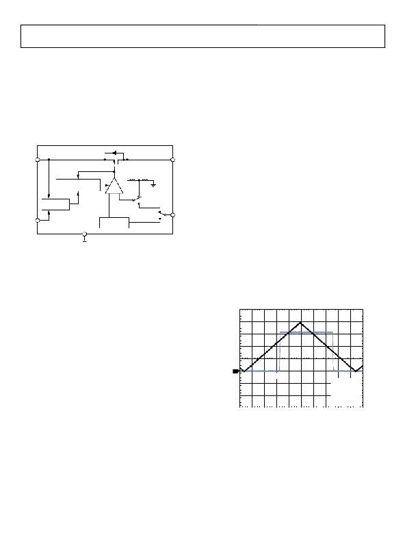
�Figure� 18.� Internal� Block� Diagram�
�Internally,� the� ADP1710/ADP1711� each� consist� of� a� reference,�
�an� error� amplifier,� a� feedback� voltage� divider,� and� a� PMOS� pass�
�transistor.� Output� current� is� delivered� via� the� PMOS� pass�
�device,� which� is� controlled� by� the� error� amplifier.� The� error�
�amplifier� compares� the� reference� voltage� with� the� feedback�
�voltage� from� the� output� and� amplifies� the� difference.� If� the�
�feedback� voltage� is� lower� than� the� reference� voltage,� the� gate� of�
�the� PMOS� device� is� pulled� lower,� allowing� more� current� to� pass�
�and� increasing� the� output� voltage.� If� the� feedback� voltage� is�
�higher� than� the� reference� voltage,� the� gate� of� the� PMOS� device�
�is� pulled� higher,� allowing� less� current� to� pass� and� decreasing� the�
�output� voltage.�
�The� ADP1710� is� available� in� two� versions,� one� with� fixed� output�
�voltage� options� and� one� with� an� adjustable� output� voltage.� The�
�must� be� connected� between� the� BYP� and� GND� pins.�
�ENABLE� FEATURE�
�The� ADP1710/ADP1711� use� the� EN� pin� to� enable� and� disable�
�the� OUT� pin� under� normal� operating� conditions.� As� shown� in�
��threshold,� OUT� turns� on.� When� a� falling� voltage� on� EN� crosses�
�the� inactive� threshold,� OUT� turns� off.�
�EN�
�2�
�fixed� output� voltage� option� is� set� internally� to� one� of� sixteen�
�values� between� 0.75� V� and� 3.3� V,� using� an� internal� feedback�
�network.� The� adjustable� output� voltage� can� be� set� to� between� 0.8�
�OUT�
�V� IN� =� 5V�
�V� OUT� =� 1.6V�
�C� IN� =� 1μF�
�C� OUT� =� 1μF�
�V� and� 5.0� V� by� an� external� voltage� divider� connected� from� OUT�
�to� ADJ.� The� ADP1711� is� available� with� fixed� output� voltage�
�options� and� features� a� bypass� pin,� which� allows� an� external�
�capacitor� to� be� connected,� which� reduces� internal� reference�
�noise.� All� devices� are� controlled� by� an� enable� pin� (EN).�
�Rev.� 0� |� Page� 8� of� 16�
�I� LOAD� =� 10mA�
�TIME� (1ms/DIV)�
�Figure� 19.� ADP1710� Adjustable� Typical� EN� Pin� Operation�
�相关PDF资料 |
PDF描述 |
|---|---|
| ADP1713AUJZ-0.9-R7 | IC REG LDO 0.9V .3A TSOT-23-5 |
| ADP1715ARMZ-R7 | IC REG LDO ADJ .5A 8MSOP |
| ADP1720ARMZ-R7 | IC REG LDO ADJ 50MA 8-MSOP |
| ADP1720TRMZ-EP | IC REG LDO ADJ 50MA 8-MSOP |
| ADP172ACBZ-2.9-R7 | IC REG LDO 2.9V .3A 4WLCSP |
相关代理商/技术参数 |
参数描述 |
|---|---|
| ADP1711-BL1-EVZ | 制造商:Analog Devices 功能描述:BLANK ADISIMPOWER EVAL ADP1711 - Boxed Product (Development Kits) |
| ADP1712 | 制造商:AD 制造商全称:Analog Devices 功能描述:evaluation boards |
| ADP1712-3.3-EVALZ | 功能描述:BOARD EVAL FOR ADP1712-3.3 RoHS:是 类别:编程器,开发系统 >> 评估板 - 线性稳压器 (LDO) 系列:- 产品变化通告:1Q2012 Discontinuation 30/Mar/2012 设计资源:NCP590MNDPTAGEVB Gerber Files 标准包装:1 系列:- 每 IC 通道数:2 - 双 输出电压:1.8V,2.8V 电流 - 输出:300mA 输入电压:2.1 ~ 5.5 V 稳压器类型:正,固定式 工作温度:-40°C ~ 85°C 板类型:完全填充 已供物品:板 已用 IC / 零件:NCP590MNDP 其它名称:NCP590MNDPTAGEVB-NDNCP590MNDPTAGEVBOS |
| ADP1712AUJZ-0.75R7 | 功能描述:IC REG LDO 0.75V .3A TSOT-23-5 RoHS:是 类别:集成电路 (IC) >> PMIC - 稳压器 - 线性 系列:- 标准包装:45 系列:- 稳压器拓扑结构:正,固定式 输出电压:5V 输入电压:6 V ~ 30 V 电压 - 压降(标准):0.47V @ 250mA 稳压器数量:1 电流 - 输出:250mA 电流 - 限制(最小):- 工作温度:-40°C ~ 125°C 安装类型:通孔 封装/外壳:TO-220-3 供应商设备封装:TO-220-3 包装:管件 产品目录页面:1289 (CN2011-ZH PDF) 其它名称:*LP2954AIT*LP2954AIT/NOPBLP2954AIT |
| ADP1712AUJZ-0.75R71 | 制造商:AD 制造商全称:Analog Devices 功能描述:300 mA, Low Dropout CMOS Linear Regulator |
发布紧急采购,3分钟左右您将得到回复。