- 您现在的位置:买卖IC网 > PDF目录20390 > ADP1864-EVALZ (Analog Devices Inc)BOARD EVALUATION ADP1864 PDF资料下载
参数资料
| 型号: | ADP1864-EVALZ |
| 厂商: | Analog Devices Inc |
| 文件页数: | 11/16页 |
| 文件大小: | 0K |
| 描述: | BOARD EVALUATION ADP1864 |
| 产品培训模块: | Power Line Monitoring |
| 标准包装: | 1 |
| 主要目的: | DC/DC,步降 |
| 输出及类型: | 1,非隔离 |
| 输出电压: | 3.3V |
| 电流 - 输出: | 3A |
| 输入电压: | 9 ~ 12V |
| 稳压器拓扑结构: | 降压 |
| 频率 - 开关: | 580kHz |
| 板类型: | 完全填充 |
| 已供物品: | 板 |
| 已用 IC / 零件: | ADP1864 |
| 产品目录页面: | 791 (CN2011-ZH PDF) |
| 相关产品: | ADP1864AUJZ-R7DKR-ND - IC REG CTRLR BUCK PWM TSOT23-6 ADP1864AUJZ-R7CT-ND - IC REG CTRLR BUCK PWM TSOT23-6 ADP1864AUJZ-R7TR-ND - IC REG CTRLR BUCK PWM TSOT23-6 |
�� �
�
�Data� Sheet�
�MOSFET�
�Choose� the� external� P-channel� MOSFET� based� on� the� following:�
�threshold� voltage� (V� T� ),� maximum� voltage� and� current� ratings,�
�R� DS(ON)� ,� and� gate� charge.�
�The� minimum� operating� voltage� of� the� ADP1864� is� 3.15� V.�
�Choose� a� MOSFET� with� a� V� T� that� is� at� least� 1� V� lower� than�
�the� minimum� input� supply� voltage� used� in� the� application.�
�Ensure� that� the� maximum� ratings� for� MOSFET� V� SG� and� V� SD� are�
�a� few� volts� greater� than� the� maximum� input� voltage� used� with�
�the� ADP1864.�
�ADP1864�
�INPUT� CAPACITOR�
�The� input� capacitor� provides� a� low� impedance� path� for� the�
�pulsed� current� drawn� by� the� external� P-channel� FET.� Choose�
�an� input� capacitor� whose� impedance� at� the� switching� frequency�
�is� lower� than� the� impedance� of� the� voltage� source� (V� IN� ).� The�
�preferred� input� capacitor� is� a� 10� μF� ceramic� capacitor� due� to�
�its� low� ESR� and� low� impedance.�
�For� all� types� of� capacitors,� make� sure� the� ripple� current� rating�
�of� the� capacitor� is� greater� than� half� of� the� maximum� output�
�load� current.�
�I� FET� (� rms� )� =�
�V� OUT� +� V� D�
�� I� LOAD�
�1�
�?�
�?� V� ?� ?� I� � ?�
�+� ESR� (10)�
�?� 8� � f� � C� C� OUT� ?�
�Estimate� the� rms� current� in� the� MOSFET� under� continuous�
�conduction� mode� by�
�V� IN� +� V� D�
�Derate� the� MOSFET� current� by� at� least� 20%� to� account� for�
�inductor� ripple� and� changes� in� the� diode� voltage.�
�The� MOSFET� power� dissipation� is� the� sum� of� the� conducted�
�and� switching� losses:�
�PD� FET(COND)� =� (� I� FET(rms)� )� 2� � (1� +� T� )� � R� DS(ON)�
�(7)�
�(8)�
�Where� space� is� limited,� multiple� capacitors� can� be� placed� in�
�parallel� to� meet� the� rms� current� requirement.� Place� the� input�
�capacitor� as� close� as� possible� to� the� IN� pin� of� the� ADP1864.�
�OUTPUT� CAPACITOR�
�The� ESR� and� capacitance� value� of� the� output� capacitor�
�determine� the� amount� of� output� voltage� ripple.�
�?� ?�
�?� OUT� ?�
�where� f� is� the� oscillator� frequency� (typically� 580� kHz).�
�1� ?� (� V� OUT� +� V� D� )� � (� V� IN� ?� V� OUT� )� ?�
�I� rms� ?� � ?�
�L� � f� � V� IN�
�2� � 3�
�?�
�?�
�where� T� =� 0.005/°C� ×� T� J� (FET)� ?� 25°C.�
�Ensure� the� maximum� power� dissipation� calculated� is� significantly�
�less� than� the� maximum� rating� of� the� MOSFET.�
�DIODE�
�The� diode� carries� the� inductor� current� during� the� off� time� of�
�Because� the� output� capacitance� is� typically� >40� μF,� the� ESR�
�dominates� the� voltage� ripple.� Ensure� the� output� capacitor�
�ripple� rating� is� greater� than� the� maximum� inductor� ripple.�
�?� ?�
�(11)�
�+� V� D�
�=� ?� 1� ?� OUT�
�?� � I� LOAD�
�I� DIODE� (� AV� )� (9)�
�V� IN� +� V� D�
�?�
�?�
�the� external� FET.� The� average� current� of� the� diode� is,� therefore,�
�dependent� on� the� duty� cycle� of� the� controller� as� well� as� the�
�output� load� current.�
�?� V� ?�
�?� ?�
�where� V� D� is� the� diode� forward� drop.�
�POSCAP?� capacitors� from� Sanyo� offer� a� good� size,� ESR,� ripple,�
�and� current� capability� trade-off.�
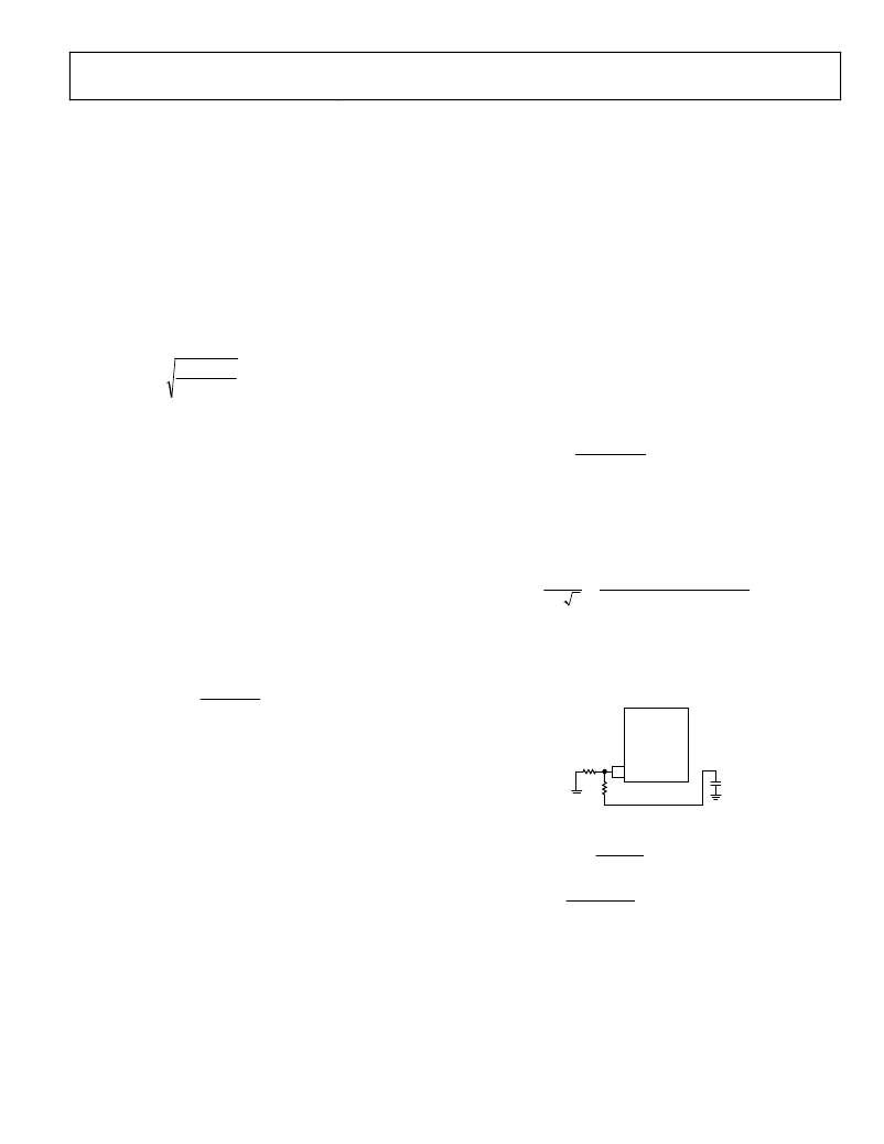
�FEEDBACK� RESISTORS�
�The� feedback� resistors� ratio� sets� the� output� voltage� of� the� system.�
�ADP1864�
�A� typical� Schottky� diode� has� a� forward� drop� voltage� of� 0.5� V.�
�A� Schottky� diode� is� recommended� for� best� efficiency� because� it�
�R2�
�3�
�R1�
�FB�
�V� OUT�
�has� a� low� forward� drop� and� faster� switching� speed� than� junction�
�diodes.� If� a� junction� diode� is� used� it� must� be� an� ultrafast� recovery�
�Figure� 14.� Two� Feedback� Resistors� Used� to� Set� Output� Voltage�
�0� .� 8� V� =� V� OUT� �
�(� V� OUT� ?� 0� .� 8� )�
�diode.� The� low� forward� drop� reduces� power� losses� during� the�
�FET� off� time,� and� fast� switching� speed� reduces� the� switching�
�losses� during� PFET� transitions.�
�R1� =� R2� �
�R� 2�
�R1� +� R� 2�
�0� .� 8�
�(12)�
�(13)�
�Choose� 80.6� k?� for� R2.� Using� higher� values� for� R2� results� in�
�reduced� output� voltage� accuracy,� and� lower� values� cause� an�
�increased� voltage� divider� current,� thus� increasing� quiescent�
�current� consumption.�
�Rev.� C� |� Page� 11� of� 16�
�相关PDF资料 |
PDF描述 |
|---|---|
| VI-B3D-CX-F1 | CONVERTER MOD DC/DC 85V 75W |
| GBA14DTAH | CONN EDGECARD 28POS R/A .125 SLD |
| MLG0603S3N0S | INDUCTOR MULTILAYER 3.0NH 0201 |
| VI-B3F-CX-F2 | CONVERTER MOD DC/DC 72V 75W |
| R0.25D12-3.324/H-R | CONV DC/DC 0.25W 3.3V +/-24VOUT |
相关代理商/技术参数 |
参数描述 |
|---|---|
| ADP1870 | 制造商:AD 制造商全称:Analog Devices 功能描述:Synchronous Buck Controller with Constant On-Time and Valley Current Mode |
| ADP1870-0.3-EVALZ | 功能描述:BOARD EVAL FOR ADP1870-0.3 RoHS:是 类别:编程器,开发系统 >> 评估板 - DC/DC 与 AC/DC(离线)SMPS 系列:* 标准包装:1 系列:- 主要目的:DC/DC,步降 输出及类型:1,非隔离 功率 - 输出:- 输出电压:3.3V 电流 - 输出:3A 输入电压:4.5 V ~ 28 V 稳压器拓扑结构:降压 频率 - 开关:250kHz 板类型:完全填充 已供物品:板 已用 IC / 零件:L7981 其它名称:497-12113STEVAL-ISA094V1-ND |
| ADP1870-0.6-EVALZ | 功能描述:BOARD EVAL FOR ADP1870-0.6 RoHS:是 类别:编程器,开发系统 >> 评估板 - DC/DC 与 AC/DC(离线)SMPS 系列:* 标准包装:1 系列:- 主要目的:DC/DC,步降 输出及类型:1,非隔离 功率 - 输出:- 输出电压:3.3V 电流 - 输出:3A 输入电压:4.5 V ~ 28 V 稳压器拓扑结构:降压 频率 - 开关:250kHz 板类型:完全填充 已供物品:板 已用 IC / 零件:L7981 其它名称:497-12113STEVAL-ISA094V1-ND |
| ADP1870-1.0-EVALZ | 功能描述:BOARD EVAL FOR ADP1870-1.0 RoHS:是 类别:编程器,开发系统 >> 评估板 - DC/DC 与 AC/DC(离线)SMPS 系列:* 标准包装:1 系列:- 主要目的:DC/DC,步降 输出及类型:1,非隔离 功率 - 输出:- 输出电压:3.3V 电流 - 输出:3A 输入电压:4.5 V ~ 28 V 稳压器拓扑结构:降压 频率 - 开关:250kHz 板类型:完全填充 已供物品:板 已用 IC / 零件:L7981 其它名称:497-12113STEVAL-ISA094V1-ND |
| ADP1870ACPZ-0.3-R7 | 功能描述:IC REG CTRLR BUCK PWM CM 10LFCSP RoHS:是 类别:集成电路 (IC) >> PMIC - 稳压器 - DC DC 切换控制器 系列:- 标准包装:2,500 系列:- PWM 型:电流模式 输出数:1 频率 - 最大:500kHz 占空比:96% 电源电压:4 V ~ 36 V 降压:无 升压:是 回扫:无 反相:无 倍增器:无 除法器:无 Cuk:无 隔离:无 工作温度:-40°C ~ 125°C 封装/外壳:24-WQFN 裸露焊盘 包装:带卷 (TR) |
发布紧急采购,3分钟左右您将得到回复。