- 您现在的位置:买卖IC网 > PDF目录20390 > ADP1864-EVALZ (Analog Devices Inc)BOARD EVALUATION ADP1864 PDF资料下载
参数资料
| 型号: | ADP1864-EVALZ |
| 厂商: | Analog Devices Inc |
| 文件页数: | 5/16页 |
| 文件大小: | 0K |
| 描述: | BOARD EVALUATION ADP1864 |
| 产品培训模块: | Power Line Monitoring |
| 标准包装: | 1 |
| 主要目的: | DC/DC,步降 |
| 输出及类型: | 1,非隔离 |
| 输出电压: | 3.3V |
| 电流 - 输出: | 3A |
| 输入电压: | 9 ~ 12V |
| 稳压器拓扑结构: | 降压 |
| 频率 - 开关: | 580kHz |
| 板类型: | 完全填充 |
| 已供物品: | 板 |
| 已用 IC / 零件: | ADP1864 |
| 产品目录页面: | 791 (CN2011-ZH PDF) |
| 相关产品: | ADP1864AUJZ-R7DKR-ND - IC REG CTRLR BUCK PWM TSOT23-6 ADP1864AUJZ-R7CT-ND - IC REG CTRLR BUCK PWM TSOT23-6 ADP1864AUJZ-R7TR-ND - IC REG CTRLR BUCK PWM TSOT23-6 |
�� ��
��
��Data� Sheet�
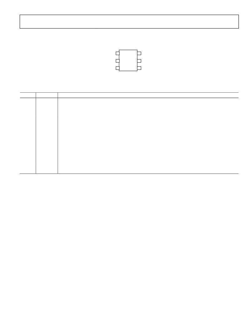
�PIN� CONFIGURATION� AND� FUNCTION� DESCRIPTIONS�
�ADP1864�
�COMP� 1�
�ADP1864�
�6�
�PGATE�
�GND� 2�
�TOP� VIEW�
�5�
�IN�
�(Not� to� Scale)�
�FB� 3�
�4�
�CS�
�Figure� 2.� Pin� Configuration�
�Table� 3.� Pin Function� Descriptions�
�Pin� No.�
�1�
�2�
�3�
�4�
�5�
�6�
�Mnemonic�
�COMP�
�GND�
�FB�
�CS�
�IN�
�PGATE�
�Description�
�Regulator� Compensation� Node.� COMP� is� the� output� of� the� internal� transconductance� error� amplifier.� Connect� a�
�series� RC� from� COMP� to� GND� to� compensate� for� the� control� loop.� Add� an� extra� high� frequency� capacitor� between�
�COMP� and� GND� to� further� reduce� switching� jitter.� The� value� of� this� is� typically� one-tenth� of� the� main� compensation�
�capacitor.� Pulling� the� COMP� pin� below� 0.3� V� disables� the� ADP1864� and� turns� off� the� external� PFET.�
�Analog� Ground.� Directly� connect� the� compensation� and� feedback� networks� to� GND,� preferably� with� a� small� analog�
�GND� plane.� Connect� GND� to� the� power� ground� (PGND)� plane� with� a� narrow� track� at� a� single� point� close� to� the� GND�
�pin.� See� the� Layout� Considerations� section� for� more� information.�
�Feedback� Input.� Connect� a� resistive� voltage� divider� from� the� output� voltage� to� FB� to� set� the� output� voltage.� The�
�regulation� feedback� voltage� is� 0.8� V.� Place� the� feedback� resistors� as� close� as� possible� to� the� FB� pin.�
�Current� Sense� Input.� CS� is� the� negative� input� of� the� current� sense� amplifier.� It� provides� the� current� feedback� signal�
�used� to� terminate� the� PWM� on� time.� Place� a� current� sense� resistor� between� IN� and� CS� to� set� the� current� limit.� The�
�current� limit� threshold� is� typically� 125� mV.�
�Power� Input.� IN� is� the� power� supply� to� the� ADP1864� and� the� positive� input� of� the� current� sense� amplifier.� Connect�
�IN� to� the� positive� side� of� the� input� voltage� source.� Bypass� IN� to� PGND� with� a� 10� μF� or� larger� capacitor� as� close� as� possible�
�to� the� ADP1864.� For� additional� high� frequency� noise� reduction,� add� a� 0.1� μF� capacitor� to� PGND� at� the� IN� pin.�
�Gate� Drive� Output.� PGATE� drives� the� gate� of� the� external� P-channel� MOSFET.� Connect� PGATE� to� the� gate� of� the�
�external� MOSFET.�
�Rev.� C� |� Page� 5� of� 16�
�相关PDF资料 |
PDF描述 |
|---|---|
| VI-B3D-CX-F1 | CONVERTER MOD DC/DC 85V 75W |
| GBA14DTAH | CONN EDGECARD 28POS R/A .125 SLD |
| MLG0603S3N0S | INDUCTOR MULTILAYER 3.0NH 0201 |
| VI-B3F-CX-F2 | CONVERTER MOD DC/DC 72V 75W |
| R0.25D12-3.324/H-R | CONV DC/DC 0.25W 3.3V +/-24VOUT |
相关代理商/技术参数 |
参数描述 |
|---|---|
| ADP1870 | 制造商:AD 制造商全称:Analog Devices 功能描述:Synchronous Buck Controller with Constant On-Time and Valley Current Mode |
| ADP1870-0.3-EVALZ | 功能描述:BOARD EVAL FOR ADP1870-0.3 RoHS:是 类别:编程器,开发系统 >> 评估板 - DC/DC 与 AC/DC(离线)SMPS 系列:* 标准包装:1 系列:- 主要目的:DC/DC,步降 输出及类型:1,非隔离 功率 - 输出:- 输出电压:3.3V 电流 - 输出:3A 输入电压:4.5 V ~ 28 V 稳压器拓扑结构:降压 频率 - 开关:250kHz 板类型:完全填充 已供物品:板 已用 IC / 零件:L7981 其它名称:497-12113STEVAL-ISA094V1-ND |
| ADP1870-0.6-EVALZ | 功能描述:BOARD EVAL FOR ADP1870-0.6 RoHS:是 类别:编程器,开发系统 >> 评估板 - DC/DC 与 AC/DC(离线)SMPS 系列:* 标准包装:1 系列:- 主要目的:DC/DC,步降 输出及类型:1,非隔离 功率 - 输出:- 输出电压:3.3V 电流 - 输出:3A 输入电压:4.5 V ~ 28 V 稳压器拓扑结构:降压 频率 - 开关:250kHz 板类型:完全填充 已供物品:板 已用 IC / 零件:L7981 其它名称:497-12113STEVAL-ISA094V1-ND |
| ADP1870-1.0-EVALZ | 功能描述:BOARD EVAL FOR ADP1870-1.0 RoHS:是 类别:编程器,开发系统 >> 评估板 - DC/DC 与 AC/DC(离线)SMPS 系列:* 标准包装:1 系列:- 主要目的:DC/DC,步降 输出及类型:1,非隔离 功率 - 输出:- 输出电压:3.3V 电流 - 输出:3A 输入电压:4.5 V ~ 28 V 稳压器拓扑结构:降压 频率 - 开关:250kHz 板类型:完全填充 已供物品:板 已用 IC / 零件:L7981 其它名称:497-12113STEVAL-ISA094V1-ND |
| ADP1870ACPZ-0.3-R7 | 功能描述:IC REG CTRLR BUCK PWM CM 10LFCSP RoHS:是 类别:集成电路 (IC) >> PMIC - 稳压器 - DC DC 切换控制器 系列:- 标准包装:2,500 系列:- PWM 型:电流模式 输出数:1 频率 - 最大:500kHz 占空比:96% 电源电压:4 V ~ 36 V 降压:无 升压:是 回扫:无 反相:无 倍增器:无 除法器:无 Cuk:无 隔离:无 工作温度:-40°C ~ 125°C 封装/外壳:24-WQFN 裸露焊盘 包装:带卷 (TR) |
发布紧急采购,3分钟左右您将得到回复。