- 您现在的位置:买卖IC网 > PDF目录15360 > ADP1871ARMZ-0.3-R7 (Analog Devices Inc)IC REG CTRLR BUCK PWM CM 10-MSOP PDF资料下载
参数资料
| 型号: | ADP1871ARMZ-0.3-R7 |
| 厂商: | Analog Devices Inc |
| 文件页数: | 6/44页 |
| 文件大小: | 0K |
| 描述: | IC REG CTRLR BUCK PWM CM 10-MSOP |
| 标准包装: | 1 |
| PWM 型: | 电流模式 |
| 输出数: | 1 |
| 频率 - 最大: | 300kHz |
| 占空比: | 84% |
| 电源电压: | 2.95 V ~ 20 V |
| 降压: | 是 |
| 升压: | 无 |
| 回扫: | 无 |
| 反相: | 无 |
| 倍增器: | 无 |
| 除法器: | 无 |
| Cuk: | 无 |
| 隔离: | 无 |
| 工作温度: | -40°C ~ 125°C |
| 封装/外壳: | 10-TFSOP,10-MSOP(0.118",3.00mm 宽) |
| 包装: | 标准包装 |
| 其它名称: | ADP1871ARMZ-0.3-R7DKR |
第1页第2页第3页第4页第5页当前第6页第7页第8页第9页第10页第11页第12页第13页第14页第15页第16页第17页第18页第19页第20页第21页第22页第23页第24页第25页第26页第27页第28页第29页第30页第31页第32页第33页第34页第35页第36页第37页第38页第39页第40页第41页第42页第43页第44页
�� ��
��
��ADP1870/ADP1871�
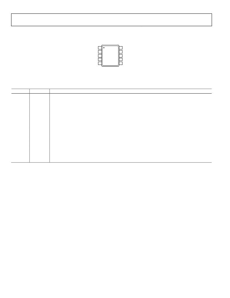
�PIN� CONFIGURATION� AND� FUNCTION� DESCRIPTIONS�
�Data� Sheet�
�VIN� 1�
�10�
�BST�
�COMP/EN� 2�
�FB� 3�
�GND� 4�
�VREG� 5�
�ADP1870/�
�ADP1871�
�TOP� VIEW�
�(Not� to� Scale)�
�9�
�8�
�7�
�6�
�SW�
�DRVH�
�PGND�
�DRVL�
�NOTES�
�1.� THE� EXPOSED� PAD� MUST� BE� CONNECTED�
�TO� GROUND.�
�Figure� 3.� Pin� Configuration�
�Table� 4.� Pin� Function� Descriptions�
�Pin� No.�
�1�
�2�
�3�
�4�
�5�
�6�
�7�
�8�
�9�
�10�
�Mnemonic�
�VIN�
�COMP/EN�
�FB�
�GND�
�VREG�
�DRVL�
�PGND�
�DRVH�
�SW�
�BST�
�Description�
�High� Input� Voltage.� Connect� VIN� to� the� drain� of� the� upper-side� MOSFET.�
�Output� of� the� Internal� Error� Amplifier/IC� Enable.� When� this� pin� functions� as� EN,� applying� 0� V� to� this� pin� disables� the� IC.�
�Noninverting� Input� of� the� Internal� Error� Amplifier.� This� is� the� node� where� the� feedback� resistor� is� connected.�
�Analog� Ground� Reference� Pin� of� the� IC.� All� sensitive� analog� components� should� be� connected� to� this� ground�
�plane� (see� the� Layout� Considerations� section).�
�Internal� Regulator� Supply� Bias� Voltage� for� the� ADP1870/ADP1871� Controller� (Includes� the� Output� Gate� Drivers).�
�A� bypass� capacitor� of� 1� μF� directly� from� this� pin� to� PGND� and� a� 0.1� μF� across� VREG� and� GND� are� recommended.�
�VREG� should� not� be� loaded� externally� because� it� is� intended� to� only� bias� internal� circuitry.�
�Drive� Output� for� the� External� Lower-Side,� N-Channel� MOSFET.� This� pin� also� serves� as� the� current-sense� gain�
��Power� GND.� Ground� for� the� lower-side� gate� driver� and� lower-side,� N-channel� MOSFET.�
�Drive� Output� for� the� External� Upper-Side,� N-Channel� MOSFET.�
�Switch� Node� Connection.�
�Bootstrap� for� the� Upper-Side� MOSFET� Gate� Drive� Circuitry.� An� internal� boot� rectifier� (diode)� is� connected�
�between� VREG� and� BST.� A� capacitor� from� BST� to� SW� is� required.� An� external� Schottky� diode� can� also� be�
�connected� between� VREG� and� BST� for� increased� gate� drive� capability.�
�Rev.� B� |� Page� 6� of� 44�
�相关PDF资料 |
PDF描述 |
|---|---|
| VI-JWX-EY-F3 | CONVERTER MOD DC/DC 5.2V 50W |
| UCS2E680MHD1TN | CAP ALUM 68UF 250V 20% RADIAL |
| VI-21D-EW-F3 | CONVERTER MOD DC/DC 85V 100W |
| HCM28DSUH | CONN EDGECARD 56POS .156 DIP SLD |
| HCM28DRUN | CONN EDGECARD 56POS .156 DIP SLD |
相关代理商/技术参数 |
参数描述 |
|---|---|
| ADP1871ARMZ-0V3-R7 | 制造商:Analog Devices 功能描述: |
| ADP1871ARMZ-0V6-R7 | 制造商:Analog Devices 功能描述: |
| ADP1871ARMZ-1.0-R7 | 功能描述:IC REG CTRLR BUCK PWM CM 10-MSOP RoHS:是 类别:集成电路 (IC) >> PMIC - 稳压器 - DC DC 切换控制器 系列:- 标准包装:2,500 系列:- PWM 型:电流模式 输出数:1 频率 - 最大:500kHz 占空比:96% 电源电压:4 V ~ 36 V 降压:无 升压:是 回扫:无 反相:无 倍增器:无 除法器:无 Cuk:无 隔离:无 工作温度:-40°C ~ 125°C 封装/外壳:24-WQFN 裸露焊盘 包装:带卷 (TR) |
| ADP1871ARMZ-1V0-R7 | 制造商:Analog Devices 功能描述: |
| ADP1871-BL1-EVZ | 功能描述:EVAL BOARD FOR ADP1871 RoHS:是 类别:编程器,开发系统 >> 评估板 - DC/DC 与 AC/DC(离线)SMPS 系列:- 标准包装:1 系列:- 主要目的:DC/DC,步降 输出及类型:1,非隔离 功率 - 输出:- 输出电压:3.3V 电流 - 输出:3A 输入电压:4.5 V ~ 28 V 稳压器拓扑结构:降压 频率 - 开关:250kHz 板类型:完全填充 已供物品:板 已用 IC / 零件:L7981 其它名称:497-12113STEVAL-ISA094V1-ND |
发布紧急采购,3分钟左右您将得到回复。