- 您现在的位置:买卖IC网 > PDF目录17427 > ADP1872-BL2-EVZ (Analog Devices Inc)EVAL BOARD FOR ADP1872 PDF资料下载
参数资料
| 型号: | ADP1872-BL2-EVZ |
| 厂商: | Analog Devices Inc |
| 文件页数: | 18/40页 |
| 文件大小: | 0K |
| 描述: | EVAL BOARD FOR ADP1872 |
| 标准包装: | 1 |
| 主要目的: | DC/DC,步降 |
| 稳压器拓扑结构: | 降压 |
| 板类型: | 裸(未填充) |
| 已供物品: | 裸板 |
| 已用 IC / 零件: | ADP1872 |
第1页第2页第3页第4页第5页第6页第7页第8页第9页第10页第11页第12页第13页第14页第15页第16页第17页当前第18页第19页第20页第21页第22页第23页第24页第25页第26页第27页第28页第29页第30页第31页第32页第33页第34页第35页第36页第37页第38页第39页第40页
�� ��
��
��ADP1872/ADP1873�
�THEORY� OF� OPERATION�
�The� ADP1872/ADP1873� are� versatile� current-mode,� synchronous�
�step-down� controllers� that� provide� superior� transient� response,�
�optimal� stability,� and� current� limit� protection� by� using� a� constant�
�on-time,� pseudo-fixed� frequency� with� a� programmable� current-�
�sense� gain,� current-control� scheme.� In� addition,� these� devices� offer�
�FB�
�ADP1872/ADP1873�
�V� DD�
�SS�
�Data� Sheet�
�optimum� performance� at� low� duty� cycles� by� using� valley� current-�
�mode� control� architecture.� This� allows� the� ADP1872/�
�COMP/EN�
�ERROR�
�AMPLIFIER�
�0.6V�
�ADP1873� to� drive� all� N-channel� power� stages� to� regulate� output�
�voltages� as� low� as� 0.6� V.�
�STARTUP�
�The� ADP1872/ADP1873� have� an� input� low� voltage� pin� (VDD)� for�
�C� C�
�R� C�
�C� C2�
�PRECISION�
�ENABLE�
�TO� ENABLE�
�ALL� BLOCKS�
�285mV�
�biasing� and� supplying� power� for� the� integrated� MOSFET� drivers.� A�
�bypass� capacitor� should� be� located� directly� across� the� VDD� (Pin� 5)�
�and� PGND� (Pin� 7)� pins.� Included� in� the� power-up� sequence� is�
�the� biasing� of� the� current-sense� amplifier,� the� current-sense� gain�
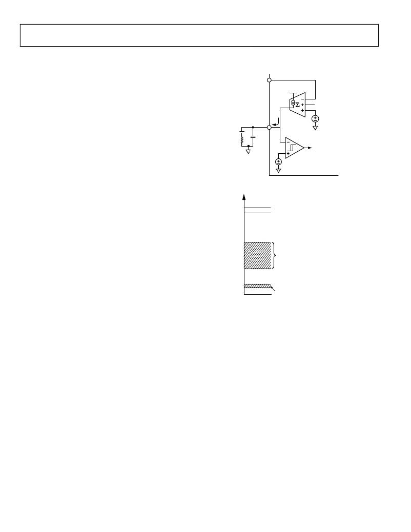
��Figure� 65.� Release� COMP/EN� Pin� to� Enable� the� ADP1872/ADP1873�
�COMP/EN�
�section),� the� soft� start� circuit,� and� the� error� amplifier.�
�The� current-sense� blocks� provide� valley� current� information�
�(see� the� Programming� Resistor� (RES)� Detect� Circuit� section)�
�and� are� a� variable� of� the� compensation� equation� for� loop� stability�
�(see� the� Compensation� Network� section).� The� valley� current�
�information� is� extracted� by� forcing� 0.4� V� across� the� DRVL� output�
�and� the� PGND� pin,� which� generates� a� current� depending� on� the�
�resistor� across� DRVL� and� PGND� in� a� process� performed� by� the�
�RES� detect� circuit.� The� current� through� the� resistor� is� used� to� set�
�the� current-sense� amplifier� gain.� This� process� takes� approximately�
�800� μs,� after� which� the� drive� signal� pulses� appear� at� the� DRVL�
�>2.4V�
�2.4V�
�1.0V�
�500mV�
�285mV�
�0V�
�HICCUP� MODE� INITIALIZED�
�MAXIMUM� CURRENT� (UPPER� CLAMP)�
�ZERO� CURRENT�
�USABLE� RANGE� ONLY� AFTER� SOFT� START�
�PERIOD� IF� CONTUNUOUS� CONDUCTION�
�MODE� OF� OPERATION� IS� SELECTED.�
�LOWER� CLAMP�
�PRECISION� ENABLE� THRESHOLD�
�35mV� HYSTERESIS�
�and� DRVH� pins� synchronously� and� the� output� voltage� begins� to�
�rise� in� a� controlled� manner� through� the� soft� start� sequence.�
�The� rise� time� of� the� output� voltage� is� determined� by� the� soft� start�
�and� error� amplifier� blocks� (see� the� Soft� Start� section).� At� the�
�beginning� of� a� soft� start,� the� error� amplifier� charges� the� external�
�compensation� capacitor,� causing� the� COMP/EN� pin� to� rise� above� the�
�enable� threshold� of� 285� mV,� thus� enabling� the� ADP1872/ADP1873.�
�SOFT� START�
�The� ADP1872/ADP1873� have� digital� soft� start� circuitry,� which�
�involves� a� counter� that� initiates� an� incremental� increase� in� current,�
�by� 1� μA,� via� a� current� source� on� every� cycle� through� a� fixed� internal�
�capacitor.� The� output� tracks� the� ramping� voltage� by� producing�
�PWM� output� pulses� to� the� upper� side� MOSFET.� The� purpose� is� to�
�limit� the� in-rush� current� from� the� high� voltage� input� supply� (VIN)�
�to� the� output� (V� OUT� ).�
�PRECISION� ENABLE� CIRCUITRY�
�The� ADP1872/ADP1873� employ� precision� enable� circuitry.� The�
�enable� threshold� is� 285� mV� typical� with� 35� mV� of� hysteresis.�
�The� devices� are� enabled� when� the� COMP/EN� pin� is� released,�
�Figure� 66.� COMP/EN� Voltage� Range�
�UNDERVOLTAGE� LOCKOUT�
�The� undervoltage� lockout� (UVLO)� feature� prevents� the� part�
�from� operating� both� the� upper� side� and� lower� side� MOSFETs�
�at� extremely� low� or� undefined� input� voltage� (VDD)� ranges.�
�Operation� at� an� undefined� bias� voltage� may� result� in� the� incorrect�
�propagation� of� signals� to� the� high-side� power� switches.� This,� in�
�turn,� results� in� invalid� output� behavior� that� can� cause� damage�
�to� the� output� devices,� ultimately� destroying� the� device� tied� at�
�the� output.� The� UVLO� level� has� been� set� at� 2.65� V� (nominal).�
�THERMAL� SHUTDOWN�
�The� thermal� shutdown� is� a� self-protection� feature� to� prevent� the� IC�
�from� damage� due� to� a� very� high� operating� junction� temperature.�
�If� the� junction� temperature� of� the� device� exceeds� 155°C,� the�
�part� enters� the� thermal� shutdown� state.� In� this� state,� the� device�
�shuts� off� both� the� upper� side� and� lower� side� MOSFETs� and�
�disables� the� entire� controller� immediately,� thus� reducing� the�
�power� consumption� of� the� IC.� The� part� resumes� operation� after�
�the� junction� temperature� of� the� part� cools� to� less� than� 140°C.�
�allowing� the� error� amplifier� output� to� rise� above� the� enable�
�threshold� (see� Figure� 65).� Grounding� this� pin� disables� the�
�ADP1872/ADP1873,� reducing� the� supply� current� of� the� devices�
��Rev.� B� |� Page� 18� of� 40�
�相关PDF资料 |
PDF描述 |
|---|---|
| MAX6133AASA30+ | IC VREF SERIES PREC 3V 8-SOIC |
| HSM03DRYN | CONN EDGECARD 6POS DIP .156 SLD |
| LQW2BAS5N6J00L | INDUCTOR RF 5.6NH 600MA 0805 |
| RSM06DTMD | CONN EDGECARD 12POS R/A .156 SLD |
| R1S12-1209-R | CONV DC/DC 1W 12VIN 09VOUT |
相关代理商/技术参数 |
参数描述 |
|---|---|
| ADP1873-0.3-EVALZ | 功能描述:BOARD EVAL FOR ADP1873-0.3 RoHS:是 类别:编程器,开发系统 >> 评估板 - DC/DC 与 AC/DC(离线)SMPS 系列:* 产品培训模块:Obsolescence Mitigation Program 标准包装:1 系列:True Shutdown™ 主要目的:DC/DC,步升 输出及类型:1,非隔离 功率 - 输出:- 输出电压:- 电流 - 输出:1A 输入电压:2.5 V ~ 5.5 V 稳压器拓扑结构:升压 频率 - 开关:3MHz 板类型:完全填充 已供物品:板 已用 IC / 零件:MAX8969 |
| ADP1873-0.6-EVALZ | 功能描述:BOARD EVAL FOR ADP1873-0.6 RoHS:是 类别:编程器,开发系统 >> 评估板 - DC/DC 与 AC/DC(离线)SMPS 系列:* 产品培训模块:Obsolescence Mitigation Program 标准包装:1 系列:True Shutdown™ 主要目的:DC/DC,步升 输出及类型:1,非隔离 功率 - 输出:- 输出电压:- 电流 - 输出:1A 输入电压:2.5 V ~ 5.5 V 稳压器拓扑结构:升压 频率 - 开关:3MHz 板类型:完全填充 已供物品:板 已用 IC / 零件:MAX8969 |
| ADP1873-1.0-EVALZ | 功能描述:BOARD EVAL FOR ADP1873-1.0 RoHS:是 类别:编程器,开发系统 >> 评估板 - DC/DC 与 AC/DC(离线)SMPS 系列:* 产品培训模块:Obsolescence Mitigation Program 标准包装:1 系列:True Shutdown™ 主要目的:DC/DC,步升 输出及类型:1,非隔离 功率 - 输出:- 输出电压:- 电流 - 输出:1A 输入电压:2.5 V ~ 5.5 V 稳压器拓扑结构:升压 频率 - 开关:3MHz 板类型:完全填充 已供物品:板 已用 IC / 零件:MAX8969 |
| ADP1873ARMZ-0.3-R7 | 功能描述:IC REG CTRLR BUCK PWM CM 10-MSOP RoHS:是 类别:集成电路 (IC) >> PMIC - 稳压器 - DC DC 切换控制器 系列:- 标准包装:2,500 系列:- PWM 型:电流模式 输出数:1 频率 - 最大:500kHz 占空比:100% 电源电压:8.2 V ~ 30 V 降压:无 升压:无 回扫:是 反相:无 倍增器:无 除法器:无 Cuk:无 隔离:是 工作温度:0°C ~ 70°C 封装/外壳:8-DIP(0.300",7.62mm) 包装:管件 产品目录页面:1316 (CN2011-ZH PDF) |
| ADP1873ARMZ-0.6-R7 | 功能描述:IC REG CTRLR BUCK PWM CM 10-MSOP RoHS:是 类别:集成电路 (IC) >> PMIC - 稳压器 - DC DC 切换控制器 系列:- 标准包装:2,500 系列:- PWM 型:电流模式 输出数:1 频率 - 最大:500kHz 占空比:100% 电源电压:8.2 V ~ 30 V 降压:无 升压:无 回扫:是 反相:无 倍增器:无 除法器:无 Cuk:无 隔离:是 工作温度:0°C ~ 70°C 封装/外壳:8-DIP(0.300",7.62mm) 包装:管件 产品目录页面:1316 (CN2011-ZH PDF) |
发布紧急采购,3分钟左右您将得到回复。