- 您现在的位置:买卖IC网 > PDF目录17427 > ADP1872-BL2-EVZ (Analog Devices Inc)EVAL BOARD FOR ADP1872 PDF资料下载
参数资料
| 型号: | ADP1872-BL2-EVZ |
| 厂商: | Analog Devices Inc |
| 文件页数: | 22/40页 |
| 文件大小: | 0K |
| 描述: | EVAL BOARD FOR ADP1872 |
| 标准包装: | 1 |
| 主要目的: | DC/DC,步降 |
| 稳压器拓扑结构: | 降压 |
| 板类型: | 裸(未填充) |
| 已供物品: | 裸板 |
| 已用 IC / 零件: | ADP1872 |
第1页第2页第3页第4页第5页第6页第7页第8页第9页第10页第11页第12页第13页第14页第15页第16页第17页第18页第19页第20页第21页当前第22页第23页第24页第25页第26页第27页第28页第29页第30页第31页第32页第33页第34页第35页第36页第37页第38页第39页第40页
�� �
�
�ADP1872/ADP1873�
�Data� Sheet�
�t� ON�
�C�
�SW�
�INFORMATION�
�I�
�VDD�
�R� (TRIMMED)�
�VIN�
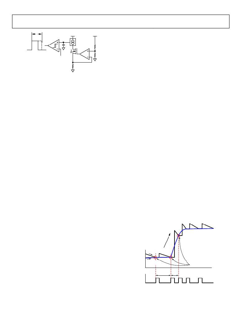
�To� illustrate� this� feature� more� clearly,� this� section� describes�
�one� such� load� transient� event—a� positive� load� step—in� detail.�
�During� load� transient� events,� the� high-side� driver� output� pulse�
�width� stays� relatively� consistent� from� cycle� to� cycle;� however,�
�the� off-time� (DRVL� on-time)� dynamically� adjusts� according� to�
�the� instantaneous� changes� in� the� external� conditions� mentioned.�
�When� a� positive� load� step� occurs,� the� error� amplifier� (out� of�
�phase� of� the� output,� V� OUT� )� produces� new� voltage� information�
�Figure� 76.� Constant� On-Time� Timer�
�The� constant� on-time� (t� ON� )� is� not� strictly� constant� because� it� varies�
�with� VIN� and� V� OUT� .� However,� this� variation� occurs� in� such� a�
�way� as� to� keep� the� switching� frequency� virtually� independent�
�of� VIN� and� V� OUT� .�
�The� t� ON� timer� uses� a� feedforward� technique,� applied� to� the� constant�
�on-time� control� loop,� making� it� pseudo-fixed� frequency� to� a� first�
�order.� Second-order� effects,� such� as� dc� losses� in� the� external� power�
�MOSFETs� (see� the� Efficiency� Consideration� section),� cause� some�
�variation� in� frequency� vs.� load� current� and� line� voltage.� These�
�effects� are� shown� in� Figure� 22� to� Figure� 33.� The� variations� in�
�frequency� are� much� reduced� compared� with� the� variations�
�generated� when� the� feedforward� technique� is� not� used.�
�The� feedforward� technique� establishes� the� following� relationship:�
�f� SW� =� 1/� K�
�where� f� SW� is� the� controller� switching� frequency� (300� kHz,�
�600� kHz,� and� 1.0� MHz).�
�The� t� ON� timer� senses� VIN� and� V� OUT� to� minimize� frequency� variation�
�with� VIN� and� V� OUT� as� previously� explained.� This� provides� a�
�pseudo-fixed� frequency,� see� the� Pseudo-Fixed� Frequency� section�
�for� additional� information.� To� allow� headroom� for� VIN/V� OUT�
�sensing,� the� following� two� equations� must� be� adhered� to.� For�
�typical� applications� where� V� DD� is� 5� V,� these� equations� are� not�
�relevant;� however,� for� lower� V� DD� ,� care� may� be� required.�
�V� DD� ≥� VIN� /8� +� 1.5�
�V� DD� ≥� V� OUT� /4�
�PSEUDO-FIXED� FREQUENCY�
�The� ADP1872/ADP1873� employ� a� constant� on-time� control�
�scheme.� During� steady� state� operation,� the� switching� frequency�
�stays� relatively� constant,� or� pseudo-fixed.� This� is� due� to� the� one-�
�shot� t� ON� timer� that� produces� a� high-side� PWM� pulse� with� a� fixed�
�duration,� given� that� external� conditions� such� as� input� voltage,�
�output� voltage,� and� load� current� are� also� at� steady� state.� During�
�load� transients,� the� frequency� momentarily� changes� for� the�
�duration� of� the� transient� event� so� that� the� output� comes� back�
�at� its� output� (COMP).� In� addition,� the� current-sense� amplifier�
�senses� new� inductor� current� information� during� this� positive�
�load� transient� event.� The� error� amplifier’s� output� voltage�
�reaction� is� compared� to� the� new� inductor� current� information�
�that� sets� the� start� of� the� next� switching� cycle.� Because� current�
�information� is� produced� from� valley� current� sensing,� it� is� sensed�
�at� the� down� ramp� of� the� inductor� current,� whereas� the� voltage�
�loop� information� is� sensed� through� the� counter� action� upswing�
�of� the� error� amplifier’s� output� (COMP).�
��which� allows� an� instantaneous� increase� in� switching� frequency�
�during� the� positive� load� transient� event.� In� summary,� a� positive�
�load� step� causes� V� OUT� to� transient� down,� which� causes� COMP� to�
�transient� up� and� therefore� shortens� the� off� time.� This� resulting�
�increase� in� frequency� during� a� positive� load� transient� helps� to�
�quickly� bring� V� OUT� back� up� in� value� and� within� the� regulation�
�window.�
�Similarly,� a� negative� load� step� causes� the� off� time� to� lengthen� in�
�response� to� V� OUT� rising.� This� effectively� increases� the� inductor�
�demagnetizing� phase,� helping� to� bring� V� OUT� to� within� regulation.�
�In� this� case,� the� switching� frequency� decreases,� or� experiences� a�
�foldback,� to� help� facilitate� output� voltage� recovery.�
�Because� the� ADP1872/ADP1873� has� the� ability� to� respond�
�rapidly� to� sudden� changes� in� load� demand,� the� recovery� period�
�in� which� the� output� voltage� settles� back� to� its� original� steady�
�state� operating� point� is� much� quicker� than� it� would� be� for� a�
�fixed-frequency� equivalent� .� Therefore,� using� a� pseudo-fixed�
�frequency,� results� in� significantly� better� load� transient�
�performance� than� using� a� fixed� frequency.�
�LOAD� CURRENT�
�DEMAND�
�CS� AMP�
�OUTPUT�
�ERROR� AMP�
�within� regulation� quicker� than� if� the� frequency� were� fixed� or� if�
�OUTPUT�
�VALLEY�
�TRIP� POINTS�
�it� were� to� remain� unchanged.� After� the� transient� event� is� complete,�
�the� frequency� returns� to� a� pseudo-fixed� value� to� a� first-order.�
�PWM� OUTPUT�
�f� SW�
�>� f� SW�
�Figure� 77.� Load� Transient� Response� Operation�
�Rev.� B� |� Page� 22� of� 40�
�相关PDF资料 |
PDF描述 |
|---|---|
| MAX6133AASA30+ | IC VREF SERIES PREC 3V 8-SOIC |
| HSM03DRYN | CONN EDGECARD 6POS DIP .156 SLD |
| LQW2BAS5N6J00L | INDUCTOR RF 5.6NH 600MA 0805 |
| RSM06DTMD | CONN EDGECARD 12POS R/A .156 SLD |
| R1S12-1209-R | CONV DC/DC 1W 12VIN 09VOUT |
相关代理商/技术参数 |
参数描述 |
|---|---|
| ADP1873-0.3-EVALZ | 功能描述:BOARD EVAL FOR ADP1873-0.3 RoHS:是 类别:编程器,开发系统 >> 评估板 - DC/DC 与 AC/DC(离线)SMPS 系列:* 产品培训模块:Obsolescence Mitigation Program 标准包装:1 系列:True Shutdown™ 主要目的:DC/DC,步升 输出及类型:1,非隔离 功率 - 输出:- 输出电压:- 电流 - 输出:1A 输入电压:2.5 V ~ 5.5 V 稳压器拓扑结构:升压 频率 - 开关:3MHz 板类型:完全填充 已供物品:板 已用 IC / 零件:MAX8969 |
| ADP1873-0.6-EVALZ | 功能描述:BOARD EVAL FOR ADP1873-0.6 RoHS:是 类别:编程器,开发系统 >> 评估板 - DC/DC 与 AC/DC(离线)SMPS 系列:* 产品培训模块:Obsolescence Mitigation Program 标准包装:1 系列:True Shutdown™ 主要目的:DC/DC,步升 输出及类型:1,非隔离 功率 - 输出:- 输出电压:- 电流 - 输出:1A 输入电压:2.5 V ~ 5.5 V 稳压器拓扑结构:升压 频率 - 开关:3MHz 板类型:完全填充 已供物品:板 已用 IC / 零件:MAX8969 |
| ADP1873-1.0-EVALZ | 功能描述:BOARD EVAL FOR ADP1873-1.0 RoHS:是 类别:编程器,开发系统 >> 评估板 - DC/DC 与 AC/DC(离线)SMPS 系列:* 产品培训模块:Obsolescence Mitigation Program 标准包装:1 系列:True Shutdown™ 主要目的:DC/DC,步升 输出及类型:1,非隔离 功率 - 输出:- 输出电压:- 电流 - 输出:1A 输入电压:2.5 V ~ 5.5 V 稳压器拓扑结构:升压 频率 - 开关:3MHz 板类型:完全填充 已供物品:板 已用 IC / 零件:MAX8969 |
| ADP1873ARMZ-0.3-R7 | 功能描述:IC REG CTRLR BUCK PWM CM 10-MSOP RoHS:是 类别:集成电路 (IC) >> PMIC - 稳压器 - DC DC 切换控制器 系列:- 标准包装:2,500 系列:- PWM 型:电流模式 输出数:1 频率 - 最大:500kHz 占空比:100% 电源电压:8.2 V ~ 30 V 降压:无 升压:无 回扫:是 反相:无 倍增器:无 除法器:无 Cuk:无 隔离:是 工作温度:0°C ~ 70°C 封装/外壳:8-DIP(0.300",7.62mm) 包装:管件 产品目录页面:1316 (CN2011-ZH PDF) |
| ADP1873ARMZ-0.6-R7 | 功能描述:IC REG CTRLR BUCK PWM CM 10-MSOP RoHS:是 类别:集成电路 (IC) >> PMIC - 稳压器 - DC DC 切换控制器 系列:- 标准包装:2,500 系列:- PWM 型:电流模式 输出数:1 频率 - 最大:500kHz 占空比:100% 电源电压:8.2 V ~ 30 V 降压:无 升压:无 回扫:是 反相:无 倍增器:无 除法器:无 Cuk:无 隔离:是 工作温度:0°C ~ 70°C 封装/外壳:8-DIP(0.300",7.62mm) 包装:管件 产品目录页面:1316 (CN2011-ZH PDF) |
发布紧急采购,3分钟左右您将得到回复。