- 您现在的位置:买卖IC网 > PDF目录14214 > ADP2102YCPZ-1.25R7 (Analog Devices Inc)IC REG BUCK SYNC 1.25V 8LFCSP PDF资料下载
参数资料
| 型号: | ADP2102YCPZ-1.25R7 |
| 厂商: | Analog Devices Inc |
| 文件页数: | 22/24页 |
| 文件大小: | 0K |
| 描述: | IC REG BUCK SYNC 1.25V 8LFCSP |
| 产品培训模块: | ADP2102 DSP Battery Life Applications |
| 标准包装: | 1 |
| 类型: | 降压(降压) |
| 输出类型: | 固定 |
| 输出数: | 1 |
| 输出电压: | 1.25V |
| 输入电压: | 2.7 V ~ 5.5 V |
| PWM 型: | 电流模式 |
| 频率 - 开关: | 3MHz |
| 电流 - 输出: | 600mA |
| 同步整流器: | 是 |
| 工作温度: | -40°C ~ 85°C |
| 安装类型: | 表面贴装 |
| 封装/外壳: | 8-VFDFN 裸露焊盘,CSP |
| 包装: | 标准包装 |
| 供应商设备封装: | 8-LFCSP-VD(3x3) |
| 其它名称: | ADP2102YCPZ-1.25R7DKR |
�� ��
��
��ADP2102�
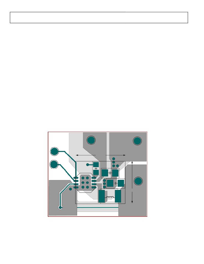
�CIRCUIT� BOARD� LAYOUT� RECOMMENDATIONS�
�Good� circuit� board� layout� is� essential� in� obtaining� the� best�
�performance� from� the� ADP2102.� Poor� circuit� layout� degrades�
�the� output� ripple� and� regulation,� as� well� as� the� EMI� and�
�electromagnetic� compatibility� performance.�
��the� typical� applications� circuit� shown� in� Figure� 48.� Use� this�
�layout� to� achieve� the� highest� performance.� Refer� to� the� following�
�guidelines� for� optimum� layout:�
�?� Use� separate� analog� and� power� ground� planes.� Connect� the�
�ground� reference� of� sensitive� analog� circuitry,� such� as� output�
�voltage� divider� components,� to� analog� ground.� In� addition,�
�connect� the� ground� references� of� power� components,� such� as�
�input� and� output� capacitors,� to� power� ground.� Connect� both�
�ground� planes� to� the� exposed� pad� of� the� ADP2102.�
�?� Place� the� input� capacitor� as� close� to� the� PVIN� pin� as� possible�
�and� connect� the� other� end� to� the� closest� power� ground� plane.�
�?� For� low� noise� and� better� transient� performance,� a� filter� is�
�recommended� between� PVIN� and� AVIN.� Place� the� 0.1� μF,�
�10� Ω� low-pass� input� filter� between� the� AVIN� pin� and� the�
�PVIN� pin,� as� close� to� AVIN� as� possible;� or� the� AVIN� pin� can�
�be� bypassed� with� a� ≥1� pF� capacitor� to� the� nearest� GND� plane.�
�RECOMMENDED� LAYOUT�
�VIN�
�?�
�?�
�Ensure� that� the� high� current� loops� are� as� short� and� as� wide�
�as� possible.� Make� the� high� current� path� from� C� IN� through� L,�
�C� OUT� ,� and� the� PGND� plane� back� to� C� IN� as� short� as� possible.�
�To� accomplish� this,� ensure� that� the� input� and� output� capacitors�
�share� a� common� PGND� plane.� In� addition,� make� the� high�
�current� path� from� the� PGND� pin� through� L� and� C� OUT� back�
�to� the� PGND� plane� as� short� as� possible.� To� do� this,� ensure�
�that� the� PGND� pin� of� the� ADP2102� is� tied� to� the� PGND�
�plane� as� close� as� possible� to� the� input� and� output� capacitors.�
�Place� the� feedback� resistor� divider� network� as� close� as� possible�
�to� the� FB� pin� to� prevent� noise� pickup.� Try� to� minimize� the�
�length� of� trace� connecting� the� top� of� the� feedback� resistor�
�divider� to� the� output� while� keeping� away� from� the� high�
�current� traces� and� the� switch� node� (LX)� that� can� lead� to�
�noise� pickup.� To� reduce� noise� pickup,� place� an� analog� ground�
�plane� on� either� side� of� the� FB� trace� and� make� it� as� small� as�
�possible� to� reduce� the� parasitic� capacitance� pickup.�
�PGND�
�MODE�
�9� mm�
�EN�
�CBP�
�CIN�
�COUT�
�VOUT�
�FB/OUT�
�8� mm�
�AGND�
�ADP2102�
�L1�
�INDUCTOR�
�Figure� 51.� Recommended� PCB� Layout� of� the� ADP2102-FXD�
�Rev.� B� |� Page� 22� of� 24�
�相关PDF资料 |
PDF描述 |
|---|---|
| EBA30DTKT | CONN EDGECARD 60POS DIP .125 SLD |
| VE-JW4-CZ-F3 | CONVERTER MOD DC/DC 48V 25W |
| MAX6865UK43D4S+T | IC MPU SUPERVISOR SOT23-5 |
| VE-JW4-CZ-F1 | CONVERTER MOD DC/DC 48V 25W |
| ABM08DTKN | CONN EDGECARD 16POS DIP .156 SLD |
相关代理商/技术参数 |
参数描述 |
|---|---|
| ADP2102YCPZ-1-R7 | 功能描述:IC REG BUCK SYNC ADJ 0.6A 8LFCSP RoHS:是 类别:集成电路 (IC) >> PMIC - 稳压器 - DC DC 开关稳压器 系列:- 标准包装:500 系列:- 类型:切换式电容器(充电泵),反相 输出类型:固定 输出数:1 输出电压:-3V 输入电压:2.3 V ~ 5.5 V PWM 型:Burst Mode? 频率 - 开关:900kHz 电流 - 输出:100mA 同步整流器:无 工作温度:-40°C ~ 85°C 安装类型:表面贴装 封装/外壳:SOT-23-6 细型,TSOT-23-6 包装:带卷 (TR) 供应商设备封装:TSOT-23-6 其它名称:LTC1983ES6-3#TRMTR |
| ADP2102YCPZ-2-R7 | 功能描述:IC REG BUCK SYNC ADJ 0.6A 8LFCSP RoHS:是 类别:集成电路 (IC) >> PMIC - 稳压器 - DC DC 开关稳压器 系列:- 标准包装:500 系列:- 类型:切换式电容器(充电泵),反相 输出类型:固定 输出数:1 输出电压:-3V 输入电压:2.3 V ~ 5.5 V PWM 型:Burst Mode? 频率 - 开关:900kHz 电流 - 输出:100mA 同步整流器:无 工作温度:-40°C ~ 85°C 安装类型:表面贴装 封装/外壳:SOT-23-6 细型,TSOT-23-6 包装:带卷 (TR) 供应商设备封装:TSOT-23-6 其它名称:LTC1983ES6-3#TRMTR |
| ADP2102YCPZ-3 | 制造商:Analog Devices 功能描述:V REG 3V 3MHZ SMD LFCSP-8 2102 |
| ADP2102YCPZ-3-R7 | 功能描述:IC REG BUCK SYNC ADJ 0.6A 8LFCSP RoHS:是 类别:集成电路 (IC) >> PMIC - 稳压器 - DC DC 开关稳压器 系列:- 产品培训模块:Lead (SnPb) Finish for COTS Obsolescence Mitigation Program 标准包装:50 系列:- 类型:升压(升压) 输出类型:两者兼有 输出数:1 输出电压:5V,2 V ~ 16.5 V 输入电压:2 V ~ 16.5 V PWM 型:- 频率 - 开关:45kHz 电流 - 输出:50mA 同步整流器:无 工作温度:0°C ~ 70°C 安装类型:通孔 封装/外壳:8-DIP(0.300",7.62mm) 包装:管件 供应商设备封装:8-PDIP |
| ADP2102YCPZ-4-R7 | 功能描述:IC REG BUCK SYNC ADJ 0.6A 8LFCSP RoHS:是 类别:集成电路 (IC) >> PMIC - 稳压器 - DC DC 开关稳压器 系列:- 产品培训模块:Lead (SnPb) Finish for COTS Obsolescence Mitigation Program 标准包装:50 系列:- 类型:升压(升压) 输出类型:两者兼有 输出数:1 输出电压:5V,2 V ~ 16.5 V 输入电压:2 V ~ 16.5 V PWM 型:- 频率 - 开关:45kHz 电流 - 输出:50mA 同步整流器:无 工作温度:0°C ~ 70°C 安装类型:通孔 封装/外壳:8-DIP(0.300",7.62mm) 包装:管件 供应商设备封装:8-PDIP |
发布紧急采购,3分钟左右您将得到回复。