- 您现在的位置:买卖IC网 > PDF目录14527 > ADP2102YCPZ-3-R7 (Analog Devices Inc)IC REG BUCK SYNC ADJ 0.6A 8LFCSP PDF资料下载
参数资料
| 型号: | ADP2102YCPZ-3-R7 |
| 厂商: | Analog Devices Inc |
| 文件页数: | 4/24页 |
| 文件大小: | 0K |
| 描述: | IC REG BUCK SYNC ADJ 0.6A 8LFCSP |
| 产品培训模块: | ADP2102 DSP Battery Life Applications |
| 标准包装: | 1 |
| 类型: | 降压(降压) |
| 输出类型: | 可调式 |
| 输出数: | 1 |
| 输出电压: | 1.5 V ~ 1.88 V |
| 输入电压: | 2.7 V ~ 5.5 V |
| PWM 型: | 电流模式 |
| 频率 - 开关: | 3MHz |
| 电流 - 输出: | 600mA |
| 同步整流器: | 是 |
| 工作温度: | -40°C ~ 85°C |
| 安装类型: | 表面贴装 |
| 封装/外壳: | 8-VFDFN 裸露焊盘,CSP |
| 包装: | 标准包装 |
| 供应商设备封装: | 8-LFCSP-VD(3x3) |
| 产品目录页面: | 791 (CN2011-ZH PDF) |
| 配用: | ADP2102-4-EVALZ-ND - BOARD EVAL 2.5V-3.3V ADJ OUTPUT ADP2102-3-EVALZ-ND - BOARD EVAL 1.5V-1.875V ADJ OUTPT ADP2102-2-EVALZ-ND - BOARD EVAL 1.2V-1.5V ADJ OUTPUT ADP2102-1-EVALZ-ND - BOARD EVAL 0.8V-1.2V ADJ OUTPUT ADP2102-1.8-EVALZ-ND - BOARD EVAL FOR ADP2102-1.8 ADP2102-1.875EVALZ-ND - BOARD EVAL FOR ADP2102-1.875 ADP2102-1.5-EVALZ-ND - BOARD EVAL FOR ADP2102-1.5 ADP2102-1.375EVALZ-ND - BOARD EVAL FOR ADP2102-1.375 ADP2102-1.25-EVALZ-ND - BOARD EVAL FOR ADP2102-1.25 ADP2102-1.0-EVALZ-ND - BOARD EVAL FOR ADP2102-1.0 更多... |
| 其它名称: | ADP2102YCPZ-3-R7DKR |
�� ��
��
��ADP2102�
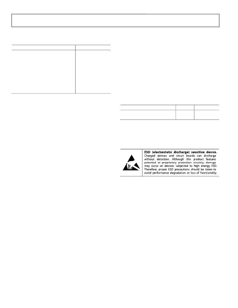
�ABSOLUTE� MAXIMUM� RATINGS�
�Table� 2.�
�THERMAL� RESISTANCE�
�Parameter�
�AVIN,� EN,� MODE,� FB/OUT� to� AGND�
�LX� to� PGND�
�PVIN� to� PGND�
�PGND� to� AGND�
�AVIN� to� PVIN�
�Operating� Ambient� Temperature� Range�
�Junction� Temperature� Range�
�Storage� Temperature� Range�
�Soldering� Conditions�
�Rating�
�?0.3� V� to� +6� V�
�?0.3� V� to� (V� IN� +� 0.3� V)�
�?0.3� V� to� +6� V�
�?0.3� V� to� +0.3� V�
�?0.3� V� to� +0.3� V�
�?40°C� to� +85°C� 1�
�?40°C� to� +125°C�
�?65°C� to� +150°C�
�JEDEC� J-STD-020�
�Junction-to-ambient� thermal� resistance� (θ� JA� )� of� the� package� is�
�based� on� modeling� and� calculation� using� a� 4-layer� board.� The�
�junction-to-ambient� thermal� resistance� is� highly� dependent� on�
�the� application� and� board� layout.� In� applications� where� high�
�maximum� power� dissipation� exists,� attention� to� thermal� board�
�design� is� required.� The� value� of� θ� JA� may� vary,� depending� on� PCB�
�material,� layout,� and� environmental� conditions.� Specified� value�
�of� θ� JA� is� based� on� a� 4-layer,� 4� in� ×� 3� in,� 2� 1/2� oz� copper� board,�
�as� per� JEDEC� standards.� For� more� information,� see� Application�
�Note� AN-772,� A� Design� and� Manufacturing� Guide� for� the� Lead�
�1�
�The� ADP2102� can� be� damaged� when� junction� temperature� limits� are� exceeded.�
�Frame� Chip� Scale� Package� (LFCSP)� .�
�Monitoring� ambient� temperature� does� not� guarantee� that� T� J� is� within� the�
�specified� temperature� limits.� In� applications� where� high� power� dissipation�
�and� poor� thermal� resistance� are� present,� the� maximum� ambient� temperature�
�may� have� to� be� derated.� In� applications� with� moderate� power� dissipation�
�and� low� PCB� thermal� resistance,� the� maximum� ambient� temperature� can�
�exceed� the� maximum� limit� as� long� as� the� junction� temperature� is� within�
�Table� 3.� Thermal� Resistance�
�Package� Type�
�8-Lead� LFCSP�
�Maximum� Power� Dissipation�
�θ� JA�
�54�
�0.74�
�Unit�
�°C/W�
�W�
�specification� limits.� The� junction� temperature� (T� J� )� of� the� device� is� dependent�
�on� the� ambient� temperature� (T� A� ),� the� power� dissipation� of� the� device� (PD),�
�and� the� junction-to-ambient� thermal� resistance� of� the� package� (θ� JA� ).� Maximum�
�junction� temperature� (T� J� )� is� calculated� from� the� ambient� temperature� (T� A� )�
�and� power� dissipation� (PD)� using� the� formula� T� J� =� T� A� +� (� θ� JA� ×� PD� ).� Unless�
�otherwise� specified,� all� other� voltages� are� referenced� to� AGND.�
�Stresses� above� those� listed� under� Absolute� Maximum� Ratings�
�may� cause� permanent� damage� to� the� device.� This� is� a� stress�
�BOUNDARY� CONDITION�
�Natural� convection,� 4-layer� board,� exposed� pad� soldered� to� PCB.�
�ESD� CAUTION�
�rating� only;� functional� operation� of� the� device� at� these� or� any�
�other� conditions� above� those� indicated� in� the� operational�
�section� of� this� specification� is� not� implied.� Exposure� to� absolute�
�maximum� rating� conditions� for� extended� periods� may� affect�
�device� reliability.�
�Rev.� B� |� Page� 4� of� 24�
�相关PDF资料 |
PDF描述 |
|---|---|
| 2200LL-390-V-RC | INDUCTOR TOROID 39UH 15% VERT |
| ESC31DREI | CONN EDGECARD 62POS .100 EYELET |
| VI-J5D-EX-S | CONVERTER MOD DC/DC 85V 75W |
| ECM31DTBI | CONN EDGECARD 62POS R/A .156 SLD |
| ABC15DRXI | CONN EDGECARD 30POS .100 DIP SLD |
相关代理商/技术参数 |
参数描述 |
|---|---|
| ADP2102YCPZ-4-R7 | 功能描述:IC REG BUCK SYNC ADJ 0.6A 8LFCSP RoHS:是 类别:集成电路 (IC) >> PMIC - 稳压器 - DC DC 开关稳压器 系列:- 产品培训模块:Lead (SnPb) Finish for COTS Obsolescence Mitigation Program 标准包装:50 系列:- 类型:升压(升压) 输出类型:两者兼有 输出数:1 输出电压:5V,2 V ~ 16.5 V 输入电压:2 V ~ 16.5 V PWM 型:- 频率 - 开关:45kHz 电流 - 输出:50mA 同步整流器:无 工作温度:0°C ~ 70°C 安装类型:通孔 封装/外壳:8-DIP(0.300",7.62mm) 包装:管件 供应商设备封装:8-PDIP |
| ADP2105 | 制造商:AD 制造商全称:Analog Devices 功能描述:1 Amp/1.5 Amp/2 Amp Synchronous, Step-Down DC-to-DC Converters |
| ADP2105-1.8-EVAL | 制造商:Analog Devices 功能描述:ADP2105-1.8 EVAL - Bulk |
| ADP2105-1.8-EVALZ | 功能描述:BOARD EVALUATION ADP2105Z 1.8V RoHS:是 类别:编程器,开发系统 >> 评估板 - DC/DC 与 AC/DC(离线)SMPS 系列:- 产品培训模块:Obsolescence Mitigation Program 标准包装:1 系列:True Shutdown™ 主要目的:DC/DC,步升 输出及类型:1,非隔离 功率 - 输出:- 输出电压:- 电流 - 输出:1A 输入电压:2.5 V ~ 5.5 V 稳压器拓扑结构:升压 频率 - 开关:3MHz 板类型:完全填充 已供物品:板 已用 IC / 零件:MAX8969 |
| ADP2105ACPZ | 制造商:Analog Devices 功能描述:V REG 1A ADJ SMD LFCSP-16 2105 |
发布紧急采购,3分钟左右您将得到回复。