- 您现在的位置:买卖IC网 > PDF目录17425 > ADP2116-BL2-EVZ (Analog Devices Inc)EVAL BOARD FOR ADP2116 PDF资料下载
参数资料
| 型号: | ADP2116-BL2-EVZ |
| 厂商: | Analog Devices Inc |
| 文件页数: | 6/36页 |
| 文件大小: | 0K |
| 描述: | EVAL BOARD FOR ADP2116 |
| 标准包装: | 1 |
| 主要目的: | DC/DC,步降 |
| 稳压器拓扑结构: | 降压 |
| 板类型: | 裸(未填充) |
| 已供物品: | 裸板 |
| 已用 IC / 零件: | ADP2116 |
第1页第2页第3页第4页第5页当前第6页第7页第8页第9页第10页第11页第12页第13页第14页第15页第16页第17页第18页第19页第20页第21页第22页第23页第24页第25页第26页第27页第28页第29页第30页第31页第32页第33页第34页第35页第36页
�� ��
��
��ADP2116�
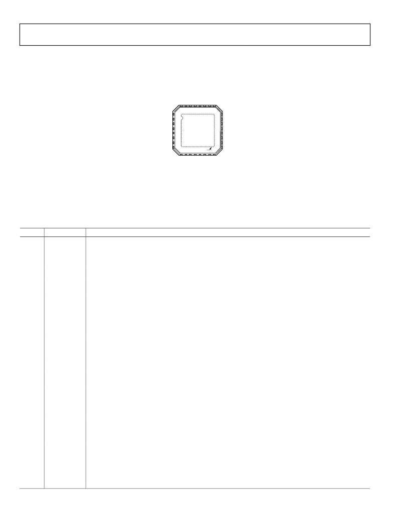
�PIN� CONFIGURATION� AND� FUNCTION� DESCRIPTIONS�
�Data� Sheet�
�GND�
�COMP1�
�1�
�2�
�24�
�23�
�SW1�
�SW2�
�FREQ�
�SCFG�
�SYNC/CLKOUT�
�OPCFG�
�COMP2�
�VDD�
�3�
�4�
�5�
�6�
�7�
�8�
�ADP2116�
�TOP� VIEW�
�(Not� to� Scale)�
�THERMAL� PAD�
�22�
�21�
�20�
�19�
�18�
�17�
�PGND1�
�PGND2�
�PGND3�
�PGND4�
�SW3�
�SW4�
�NOTES�
�1.� CONNECT� THE� EXPOSED� THERMAL� PAD� TO� THE�
�SIGNAL/ANALOG� GROUND� PLANE.�
�Figure� 3.� Pin� Configuration�
�Table� 3.� Pin� Function� Descriptions�
�Pin� No.�
�1�
�2�
�3�
�4�
�5�
�6�
�7�
�8�
�9�
�10�
�11�
�12�
�13�
�Mnemonic�
�GND�
�COMP1�
�FREQ�
�SCFG�
�SYNC/CLKOUT�
�OPCFG�
�COMP2�
�VDD�
�FB2�
�V2SET�
�SS2�
�PGOOD2�
�EN2�
�Description�
�Ground� for� the� Internal� Analog� and� Digital� Circuits.� Connect� GND� to� the� signal/analog� ground� plane� before� connecting�
�to� the� power� ground.�
�Error� Amplifier� Output� for� Channel� 1.� Connect� a� series� RC� network� from� COMP1� to� GND� to� compensate� the� control�
�loop� of� Channel� 1.� For� multiphase� operation,� tie� COMP1� and� COMP2� together.�
�Frequency� Select� Input.� Connect� this� pin� through� a� resistor� to� GND� to� set� the� appropriate� switching� frequency�
��Synchronization� Configuration� Input.� SCFG� configures� the� SYNC/CLKOUT� pin� as� an� input� or� output.� Tie� this� pin� to�
�VDD� to� configure� SYNC/CLKOUT� as� an� output.� Tie� this� pin� to� GND� to� configure� SYNC/CLKOUT� as� an� input.�
�External� Synchronization� Input/Internal� Clock� Output.� This� bidirectional� pin� is� configured� with� the� SCFG� pin� (see� the�
�Pin� 4� description� for� details).� When� this� pin� is� configured� as� an� output,� a� buffered� clock� of� twice� the� switching� frequency�
�with� a� phase� shift� of� 90°� is� available� on� this� pin.� When� configured� as� an� input,� this� pin� accepts� an� external� clock� to� which�
�the� converters� are� synchronized.� The� frequency� select� resistor,� mentioned� in� the� description� of� Pin� 3,� must� be� selected�
�to� be� close� to� the� expected� switching� frequency� for� stable� operation� (see� the� Setting� the� Oscillator� Frequency�
�section).�
�Operation� Configuration� Input.� Connect� this� pin� to� VDD� or� through� a� resistor� to� GND� to� set� the� system� mode� of�
�operation� according� to� Table� 7.� This� pin� can� be� used� to� select� a� peak� current� limit� for� each� power� channel� and� to�
�enable� or� disable� the� pulse� skip� mode.�
�Error� Amplifier� Output� for� Channel� 2.� Connect� a� series� RC� network� from� COMP2� to� GND� to� compensate� the� control�
�loop� of� Channel� 2.� For� multiphase� operation,� tie� COMP1� and� COMP2� together.�
�Power� Supply� Input.� The� power� source� for� the� ADP2116� internal� circuitry.� Connect� VDD� and� VINx� with� a� 10� Ω� resistor�
�as� close� as� possible� to� the� ADP2116.� Bypass� VDD� to� GND� with� a� 1� μF� or� greater� capacitor.�
�Feedback� Voltage� Input� for� Channel� 2.� For� the� fixed� output� voltage� option,� connect� FB2� to� V� OUT2� .� For� the� adjustable�
�output� voltage� option,� connect� this� pin� to� a� resistor� divider� between� V� OUT2� and� GND.� The� reference� voltage� for� the�
�adjustable� output� voltage� option� is� 0.6� V.� With� multiphase� configurations,� the� FB2� and� FB1� pins� should� be� tied�
�together� and� then� connected� to� V� OUT� .�
�Output� Voltage� Set� Pin� for� Channel� 2.� To� select� a� fixed� output� voltage� option� (0.8� V,� 1.2� V,� 1.5� V,� 1.8� V,� 2.5� V,� or� 3.3� V)�
�for� V� OUT2� ,� connect� this� pin� through� a� resistor� to� GND� (see� Table� 4� for� details).� To� select� an� adjustable� output� voltage�
�for� V� OUT2� ,� connect� this� pin� to� GND� through� an� 82� k� resistor� or� tie� this� pin� directly� to� VDD� depending� on� the�
�output� voltage� desired.�
�Soft� Start� Input� for� Channel� 2.� Place� a� capacitor� from� SS2� to� GND� to� set� the� soft� start� period.� A� 10� nF� capacitor�
�sets� a� 1� ms� soft� start� period.� For� multiphase� configuration,� connect� SS2� to� SS1.�
�Open-Drain� Power-Good� Output� for� Channel� 2.� Place� a� 100� k� pull-up� resistor� to� VDD� or� to� any� other� voltage� that� is�
�5.5� V� or� less;� PGOOD2� is� held� low� when� Channel� 2� is� out� of� regulation.�
�Enable� Input� for� Channel� 2.� Drive� EN2� high� to� turn� on� the� Channel� 2� converter;� drive� EN2� low� to� turn� off� the� Channel� 2�
�converter.� Tie� EN2� to� VDD� for� startup� with� VDD.� When� using� a� multiphase� configuration,� connect� EN2� to� EN1.�
�Rev.� A� |� Page� 6� of� 36�
�相关PDF资料 |
PDF描述 |
|---|---|
| CT8BK18-M | 8" BLACK 18LB CABLE TIE |
| A9CCA-0202F | FLEX CABLE - AFG02A/AF02/AFG02A |
| M7LTK-1410R | IDC CABLE - MDH14K/MC14M/MDL14K |
| MX877R | IC SW DVR 60V 8CH P-P 28-QFN |
| CT8NT50-M | 8" NATURAL 50LB CABLE TIE |
相关代理商/技术参数 |
参数描述 |
|---|---|
| ADP2116-EVALZ | 制造商:AD 制造商全称:Analog Devices 功能描述:Configurable, Dual 3 A/Single 6 A, Synchronous, Step-Down DC-to-DC Regulator |
| ADP2118 | 制造商:AD 制造商全称:Analog Devices 功能描述:3 A, 1.2 MHz/600 kHz High Efficiency Synchronous Step-Down DC-to-DC Converter |
| ADP21180001CPZR7 | 功能描述:IC REG BUCK ADJ 制造商:analog devices inc. 系列:* 零件状态:上次购买时间 标准包装:1 |
| ADP2118ACPZ-1.0-R7 | 功能描述:IC REG BUCK SYNC 1V 3A 16LFCSP RoHS:是 类别:集成电路 (IC) >> PMIC - 稳压器 - DC DC 开关稳压器 系列:- 标准包装:500 系列:- 类型:切换式电容器(充电泵),反相 输出类型:固定 输出数:1 输出电压:-3V 输入电压:2.3 V ~ 5.5 V PWM 型:Burst Mode? 频率 - 开关:900kHz 电流 - 输出:100mA 同步整流器:无 工作温度:-40°C ~ 85°C 安装类型:表面贴装 封装/外壳:SOT-23-6 细型,TSOT-23-6 包装:带卷 (TR) 供应商设备封装:TSOT-23-6 其它名称:LTC1983ES6-3#TRMTR |
| ADP2118ACPZ-1.2-R7 | 功能描述:IC REG BUCK SYNC 1.2V 3A 16LFCSP RoHS:是 类别:集成电路 (IC) >> PMIC - 稳压器 - DC DC 开关稳压器 系列:- 标准包装:250 系列:- 类型:降压(降压) 输出类型:固定 输出数:1 输出电压:1.2V 输入电压:2.05 V ~ 6 V PWM 型:电压模式 频率 - 开关:2MHz 电流 - 输出:500mA 同步整流器:是 工作温度:-40°C ~ 85°C 安装类型:表面贴装 封装/外壳:6-UFDFN 包装:带卷 (TR) 供应商设备封装:6-SON(1.45x1) 产品目录页面:1032 (CN2011-ZH PDF) 其它名称:296-25628-2 |
发布紧急采购,3分钟左右您将得到回复。