- 您现在的位置:买卖IC网 > PDF目录14225 > ADP2138ACBZ-2.8-R7 (Analog Devices Inc)IC REG BUCK SYNC 2.8V .8A 6WLCSP PDF资料下载
参数资料
| 型号: | ADP2138ACBZ-2.8-R7 |
| 厂商: | Analog Devices Inc |
| 文件页数: | 11/20页 |
| 文件大小: | 0K |
| 描述: | IC REG BUCK SYNC 2.8V .8A 6WLCSP |
| 产品变化通告: | 8mm Carrier Tape Changes 28/Feb/2012 |
| 标准包装: | 3,000 |
| 类型: | 降压(降压) |
| 输出类型: | 固定 |
| 输出数: | 1 |
| 输出电压: | 2.8V |
| 输入电压: | 2.3 V ~ 5.5 V |
| PWM 型: | 电流模式 |
| 频率 - 开关: | 3MHz |
| 电流 - 输出: | 800mA |
| 同步整流器: | 是 |
| 工作温度: | -40°C ~ 85°C |
| 安装类型: | 表面贴装 |
| 封装/外壳: | 6-UFBGA,WLCSP |
| 包装: | 带卷 (TR) |
| 供应商设备封装: | 6-WLCSP(1.03x1.50) |
�� ��
��
��Data� Sheet�
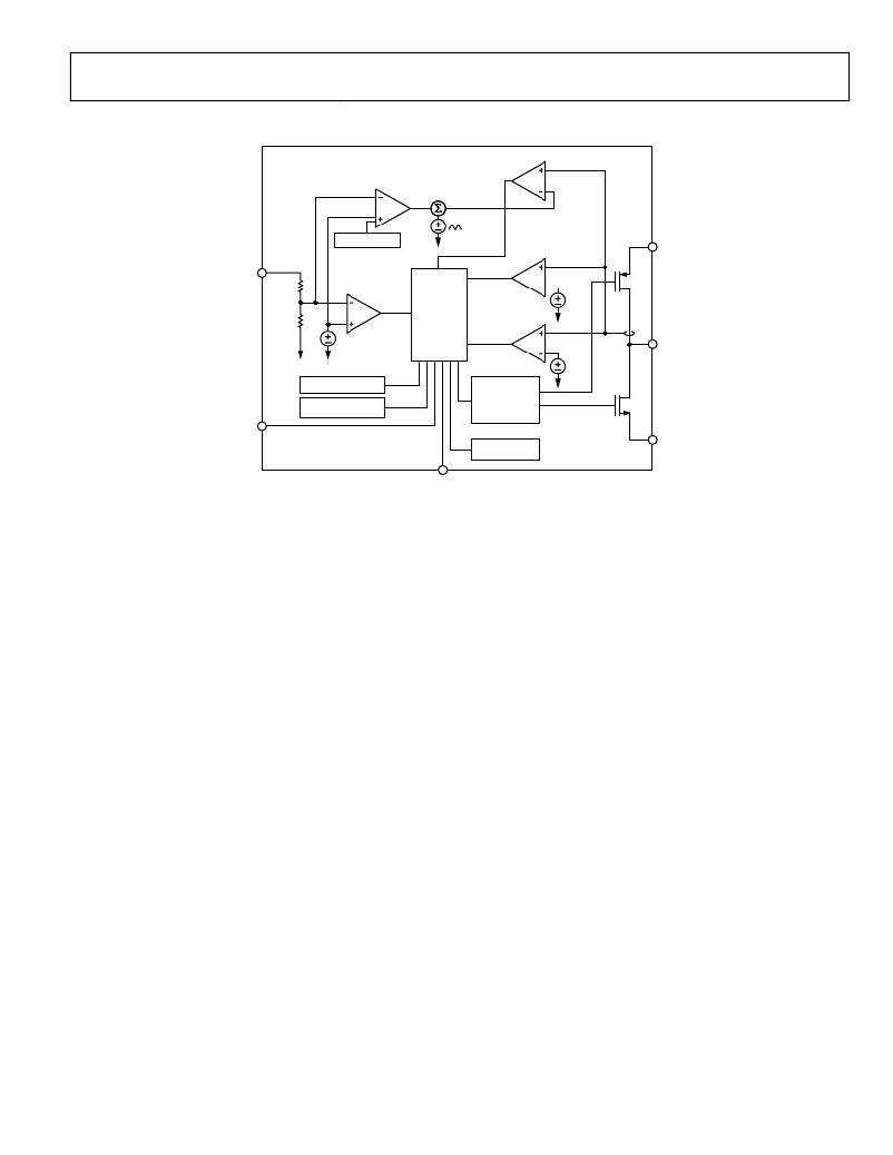
�THEORY� OF� OPERATION�
�GM� ERROR�
�AMP�
�PWM�
�COMP�
�ADP2138/ADP2139�
�VOUT�
�SOFT� START�
�PSM�
�COMP�
�PWM/�
�PSM�
�CONTROL�
�I� LIMIT�
�LOW�
�VIN�
�CURRENT�
�SW�
�MODE�
�OSCILLATOR�
�UNDERVOLTAGE�
�LOCK� OUT�
�DRIVER�
�AND�
�ANTISHOOT�
�THROUGH�
�ADP2138�
�THERMAL�
�SHUTDOWN�
�GND�
�EN�
�Figure� 33.� ADP2138� Functional� Block� Diagram�
�The� ADP2138� and� ADP2139� are� step-down� dc-to-dc� converters�
�that� use� a� fixed� frequency� and� high� speed� current-mode� archi-�
�tecture.� The� high� switching� frequency� and� tiny� 6-ball� WLCSP�
�package� allow� for� a� small� step-down� dc-to-dc� converter� solution.�
�The� ADP2138/ADP2139� operate� with� an� input� voltage� of� 2.3� V�
�to� 5.5� V,� and� regulate� an� output� voltage� down� to� 0.8� V.�
�CONTROL� SCHEME�
�The� ADP2138/ADP2139� operate� with� a� fixed� frequency,� current-�
�mode� PWM� control� architecture� at� medium� to� high� loads� for�
�high� efficiency,� but� shift� to� a� power� save� mode� control� scheme�
�at� light� loads� to� lower� the� regulation� power� losses.� When� operating�
�in� PWM� mode,� the� duty� cycle� of� the� integrated� switches� is� adjusted�
�and� regulates� the� output� voltage.� When� operating� in� power� save�
�mode� at� light� loads,� the� output� voltage� is� controlled� in� a� hyste-�
�retic� manner,� with� higher� V� OUT� ripple.� During� part� of� this� time,�
�the� converter� is� able� to� stop� switching� and� enters� an� idle� mode,�
�which� improves� conversion� efficiency.� Each� ADP2138/ADP2139�
�has� a� MODE� pin,� which� determines� the� operation� of� the� buck�
�regulator� in� either� PWM� mode� (when� the� MODE� pin� is� set�
�high)� or� power� save� mode� (when� the� mode� pin� is� set� low).�
�PWM� MODE�
�In� PWM� mode,� the� ADP2138/ADP2139� operate� at� a� fixed�
�frequency� of� 3� MHz,� set� by� an� internal� oscillator.� At� the� start�
�of� each� oscillator� cycle,� the� PFET� switch� is� turned� on,� sending�
�a� positive� voltage� across� the� inductor.� Current� in� the� inductor�
�increases� until� the� current� sense� signal� crosses� the� peak� inductor�
�current� threshold� that� turns� off� the� PFET� switch� and� turns� on�
�the� NFET� synchronous� rectifier.� This� sends� a� negative� voltage�
�across� the� inductor,� causing� the� inductor� current� to� decrease.�
�The� synchronous� rectifier� stays� on� for� the� rest� of� the� cycle.�
�The� ADP2138/ADP2139� regulate� the� output� voltage� by� adjusting�
�the� peak� inductor� current� threshold.�
�POWER� SAVE� MODE�
�The� ADP2138/ADP2139� smoothly� transition� to� the� power� save�
�mode� of� operation� when� the� load� current� decreases� below� the�
�power� save� mode� current� threshold.� When� the� ADP2138� and�
�ADP2139� enter� power� save� mode,� an� offset� is� induced� in� the� PWM�
�regulation� level,� which� makes� the� output� voltage� rise.� When� the�
�output� voltage� reaches� a� level� approximately� 1.5%� above� the� PWM�
�regulation� level,� PWM� operation� turns� off.� At� this� point,� both�
�power� switches� are� off,� and� the� ADP2138/� ADP2139� enter� into�
�idle� mode.� C� OUT� discharges� until� V� OUT� falls� to� the� PWM� regulation�
�voltage,� at� which� point� the� device� drives� the� inductor� to� cause�
�V� OUT� to� rise� again� to� the� upper� threshold.� This� process� is� repeated�
�for� as� long� as� the� load� current� is� below� the� power� save� mode�
�current� threshold.�
�Power� Save� Mode� Current� Threshold�
�The� power� save� mode� current� threshold� is� set� to� 100� mA.� The�
�ADP2138/ADP2139� employ� a� scheme� that� enables� this� current�
�to� remain� accurately� controlled,� independent� of� V� IN� and� V� OUT�
�levels.� This� scheme� also� ensures� that� there� is� very� little� hysteresis�
�between� the� power� save� mode� current� threshold� for� entry� to� and�
�exit� from� the� power� save� mode.� The� power� save� mode� current�
�threshold� is� optimized� for� excellent� efficiency� across� all� load�
�currents.�
�ENABLE/SHUTDOWN�
�The� ADP2138/ADP2139� start� operating� with� soft� start� when�
�the� EN� pin� is� toggled� from� logic� low� to� logic� high.� Pulling� the�
�EN� pin� low� forces� the� device� into� shutdown� mode,� reducing� the�
�shutdown� current� to� 0.2� μA� (typical).�
�Rev.� C� |� Page� 11� of� 20�
�相关PDF资料 |
PDF描述 |
|---|---|
| ADP2139ACBZ-2.5-R7 | IC REG BUCK SYNC 2.5V .8A 6WLCSP |
| ADP2139ACBZ-1.5-R7 | IC REG BUCK SYNC 1.5V .8A 6WLCSP |
| ADP2139ACBZ-1.0-R7 | IC REG BUCK SYNC 1V 0.8A 6WLCSP |
| ADP2139ACBZ-0.8-R7 | IC REG BUCK SYNC 0.8V .8A 6WLCSP |
| ADP2138ACBZ-3.3-R7 | IC REG BUCK SYNC 3.3V .8A 6WLCSP |
相关代理商/技术参数 |
参数描述 |
|---|---|
| ADP2138ACBZ-3.0-R7 | 功能描述:IC REG BUCK SYNC 3V 0.8A 6WLCSP RoHS:是 类别:集成电路 (IC) >> PMIC - 稳压器 - DC DC 开关稳压器 系列:- 标准包装:500 系列:- 类型:切换式电容器(充电泵),反相 输出类型:固定 输出数:1 输出电压:-3V 输入电压:2.3 V ~ 5.5 V PWM 型:Burst Mode? 频率 - 开关:900kHz 电流 - 输出:100mA 同步整流器:无 工作温度:-40°C ~ 85°C 安装类型:表面贴装 封装/外壳:SOT-23-6 细型,TSOT-23-6 包装:带卷 (TR) 供应商设备封装:TSOT-23-6 其它名称:LTC1983ES6-3#TRMTR |
| ADP2138ACBZ-3.3-R7 | 功能描述:IC REG BUCK SYNC 3.3V .8A 6WLCSP RoHS:是 类别:集成电路 (IC) >> PMIC - 稳压器 - DC DC 开关稳压器 系列:- 标准包装:500 系列:- 类型:切换式电容器(充电泵),反相 输出类型:固定 输出数:1 输出电压:-3V 输入电压:2.3 V ~ 5.5 V PWM 型:Burst Mode? 频率 - 开关:900kHz 电流 - 输出:100mA 同步整流器:无 工作温度:-40°C ~ 85°C 安装类型:表面贴装 封装/外壳:SOT-23-6 细型,TSOT-23-6 包装:带卷 (TR) 供应商设备封装:TSOT-23-6 其它名称:LTC1983ES6-3#TRMTR |
| ADP2138CB-1.8EVALZ | 功能描述:BOARD EVALUATION FOR ADP2138 RoHS:是 类别:编程器,开发系统 >> 评估板 - DC/DC 与 AC/DC(离线)SMPS 系列:- 产品培训模块:Obsolescence Mitigation Program 标准包装:1 系列:True Shutdown™ 主要目的:DC/DC,步升 输出及类型:1,非隔离 功率 - 输出:- 输出电压:- 电流 - 输出:1A 输入电压:2.5 V ~ 5.5 V 稳压器拓扑结构:升压 频率 - 开关:3MHz 板类型:完全填充 已供物品:板 已用 IC / 零件:MAX8969 |
| ADP2138CB2.85EVALZ | 功能描述:BOARD EVALUATION FOR ADP2138 RoHS:是 类别:编程器,开发系统 >> 评估板 - DC/DC 与 AC/DC(离线)SMPS 系列:- 产品培训模块:Obsolescence Mitigation Program 标准包装:1 系列:True Shutdown™ 主要目的:DC/DC,步升 输出及类型:1,非隔离 功率 - 输出:- 输出电压:- 电流 - 输出:1A 输入电压:2.5 V ~ 5.5 V 稳压器拓扑结构:升压 频率 - 开关:3MHz 板类型:完全填充 已供物品:板 已用 IC / 零件:MAX8969 |
| ADP2138CB-2.8EVALZ | 功能描述:BOARD EVALUATION FOR ADP2138 RoHS:是 类别:编程器,开发系统 >> 评估板 - DC/DC 与 AC/DC(离线)SMPS 系列:- 产品培训模块:Obsolescence Mitigation Program 标准包装:1 系列:True Shutdown™ 主要目的:DC/DC,步升 输出及类型:1,非隔离 功率 - 输出:- 输出电压:- 电流 - 输出:1A 输入电压:2.5 V ~ 5.5 V 稳压器拓扑结构:升压 频率 - 开关:3MHz 板类型:完全填充 已供物品:板 已用 IC / 零件:MAX8969 |
发布紧急采购,3分钟左右您将得到回复。