- 您现在的位置:买卖IC网 > PDF目录14225 > ADP2138ACBZ-2.8-R7 (Analog Devices Inc)IC REG BUCK SYNC 2.8V .8A 6WLCSP PDF资料下载
参数资料
| 型号: | ADP2138ACBZ-2.8-R7 |
| 厂商: | Analog Devices Inc |
| 文件页数: | 4/20页 |
| 文件大小: | 0K |
| 描述: | IC REG BUCK SYNC 2.8V .8A 6WLCSP |
| 产品变化通告: | 8mm Carrier Tape Changes 28/Feb/2012 |
| 标准包装: | 3,000 |
| 类型: | 降压(降压) |
| 输出类型: | 固定 |
| 输出数: | 1 |
| 输出电压: | 2.8V |
| 输入电压: | 2.3 V ~ 5.5 V |
| PWM 型: | 电流模式 |
| 频率 - 开关: | 3MHz |
| 电流 - 输出: | 800mA |
| 同步整流器: | 是 |
| 工作温度: | -40°C ~ 85°C |
| 安装类型: | 表面贴装 |
| 封装/外壳: | 6-UFBGA,WLCSP |
| 包装: | 带卷 (TR) |
| 供应商设备封装: | 6-WLCSP(1.03x1.50) |
�� ��
��
��ADP2138/ADP2139�
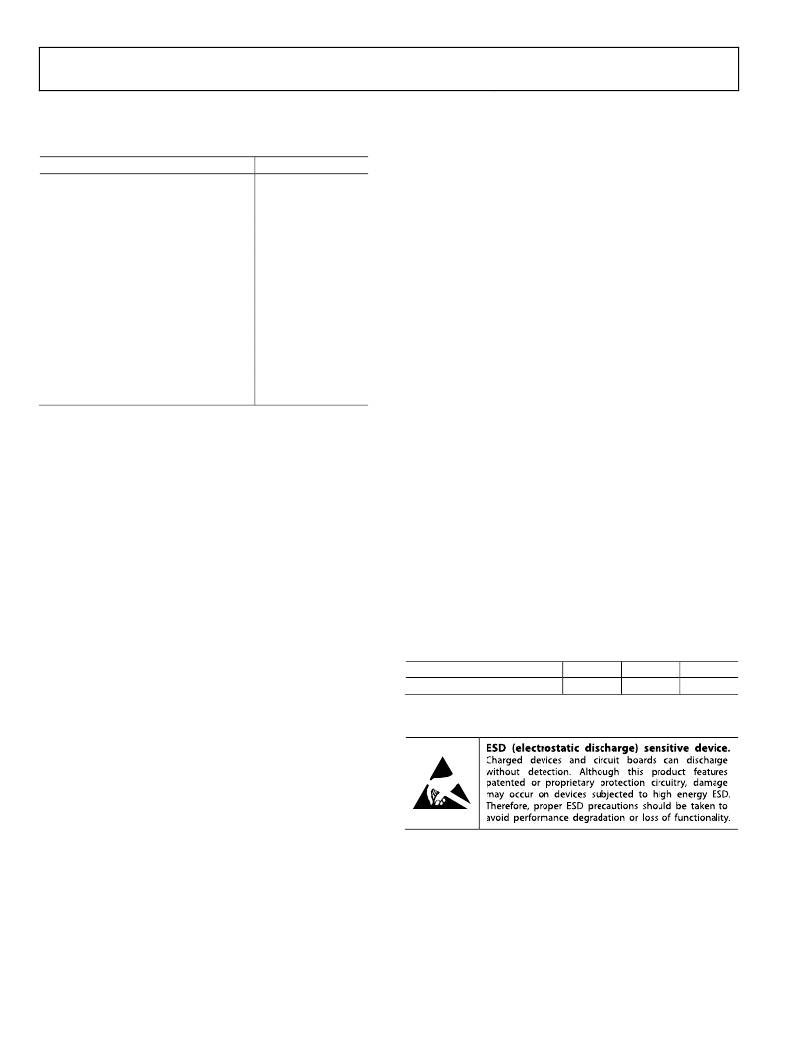
�ABSOLUTE� MAXIMUM� RATINGS�
�Data� Sheet�
�Table� 3.�
�Parameter�
�VIN,� EN,� MODE�
�VOUT,� SW� to� GND�
�Temperature� Range�
�Operating� Ambient�
�Operating� Junction�
�Storage� Temperature�
�Lead� Temperature� Range�
�Soldering� (10� sec)�
�Vapor� Phase� (60� sec)�
�Infrared� (15� sec)�
�ESD� Model�
�Human� Body�
�Charged� Device�
�Machine�
�Rating�
�?0.4� V� to� +6.5� V�
�?1.0� V� to� (V� IN� +� 0.2� V)�
�?40°C� to� +85°C�
�?40°C� to� +125°C�
�?65°C� to� +150°C�
�?65°C� to� +150°C�
�300°C�
�215°C�
�220°C�
�±1500� V�
�±500� V�
�±100� V�
�Junction-to-ambient� thermal� resistance� (θ� JA� )� of� the� package� is�
�based� on� modeling� and� calculation� using� a� 4-layer� board.� The�
�junction-to-ambient� thermal� resistance� is� highly� dependent� on�
�the� application� and� board� layout.� In� applications� where� high�
�maximum� power� dissipation� exists,� close� attention� to� thermal�
�board� design� is� required.� The� value� of� θ� JA� may� vary,� depending� on�
�PCB� material,� layout,� and� environmental� conditions.� The� specified�
�values� of� θ� JA� are� based� on� a� 4-layer,� 4� in.� ×� 3� in.,� circuit� board.� Refer�
�to� JEDEC� JESD� 51-9� for� detailed� information� pertaining� to� board�
�construction.� For� additional� information,� see� AN-617� Application�
��� JB� is� the� junction-to-board� thermal� characterization� parameter�
�measured� in� units� of� °C/W.� Ψ� JB� of� the� package� is� based� on� modeling�
�and� calculation� using� a� 4-layer� board.� The� JESD51-12,� Guidelines�
�for� Reporting� and� Using� Package� Thermal� Information� ,� states� that�
�thermal� characterization� parameters� are� not� the� same� as� thermal�
�resistances.� Ψ� JB� measures� the� component� power� flowing� through�
�Stresses� above� those� listed� under� Absolute� Maximum� Ratings�
�may� cause� permanent� damage� to� the� device.� This� is� a� stress�
�rating� only;� functional� operation� of� the� device� at� these� or� any�
�other� conditions� above� those� indicated� in� the� operational�
�section� of� this� specification� is� not� implied.� Exposure� to� absolute�
�maximum� rating� conditions� for� extended� periods� may� affect�
�device� reliability.�
�THERMAL� DATA�
�Absolute� maximum� ratings� apply� individually� only,� not� in�
�combination.�
�ADP2138/ADP2139� can� be� damaged� when� the� junction� tempera-�
�ture� limits� are� exceeded.� Monitoring� ambient� temperature� does�
�not� guarantee� that� the� junction� temperature� (T� J� )� is� within� the�
�multiple� thermal� paths� rather� than� through� a� single� path,� which�
�is� the� procedure� for� measuring� thermal� resistance,� θ� JB� .� There-�
�fore,� Ψ� JB� thermal� paths� include� convection� from� the� top� of� the�
�package� as� well� as� radiation� from� the� package;� factors� that� make�
�Ψ� JB� more� useful� in� real-world� applications� than� θ� JB� .� Maximum�
�junction� temperature� (T� J� )� is� calculated� from� the� board� temperature�
�(T� B� )� and� power� dissipation� (P� D� )� using� the� formula�
�T� J� =� T� B� +� (� P� D� ×� Ψ� JB� )�
�Refer� to� JEDEC� JESD51-8� and� JESD51-12� for� more� detailed�
�information� about� Ψ� JB� .�
�THERMAL� RESISTANCE�
�θ� JA� and� Ψ� JB� are� specified� for� the� worst-case� conditions,� that� is,� a�
�device� soldered� in� a� circuit� board� for� surface-mount� packages.�
�specified� temperature� limits.� In� applications� with� high� power�
�dissipation� and� poor� thermal� resistance,� the� maximum� ambient�
�temperature� may� need� to� be� derated.� In� applications� with� mod-�
�erate� power� dissipation� and� low� printed� circuit� board� (PCB)�
�Table� 4.� Thermal� Resistance�
�Package� Type�
�6-Ball� WLCSP�
�θ� JA�
�170�
�Ψ� JB�
�80�
�Unit�
�°C/W�
�thermal� resistance,� the� maximum� ambient� temperature� can�
�exceed� the� maximum� limit� for� as� long� as� the� junction� temperature�
�ESD� CAUTION�
�is� within� specification� limits.� The� junction� temperature� (T� J� )� of�
�the� device� is� dependent� on� the� ambient� temperature� (T� A� ),� the�
�power� dissipation� of� the� device� (P� D� ),� and� the� junction-to-ambient�
�thermal� resistance� of� the� package� (θ� JA� ).� Maximum� junction�
�temperature� (T� J� )� is� calculated� from� the� ambient� temperature�
�(T� A� )� and� power� dissipation� (P� D� )� using� the� formula�
�T� J� =� T� A� +� (� P� D� ×� θ� JA� )�
�Rev.� C� |� Page� 4� of� 20�
�相关PDF资料 |
PDF描述 |
|---|---|
| ADP2139ACBZ-2.5-R7 | IC REG BUCK SYNC 2.5V .8A 6WLCSP |
| ADP2139ACBZ-1.5-R7 | IC REG BUCK SYNC 1.5V .8A 6WLCSP |
| ADP2139ACBZ-1.0-R7 | IC REG BUCK SYNC 1V 0.8A 6WLCSP |
| ADP2139ACBZ-0.8-R7 | IC REG BUCK SYNC 0.8V .8A 6WLCSP |
| ADP2138ACBZ-3.3-R7 | IC REG BUCK SYNC 3.3V .8A 6WLCSP |
相关代理商/技术参数 |
参数描述 |
|---|---|
| ADP2138ACBZ-3.0-R7 | 功能描述:IC REG BUCK SYNC 3V 0.8A 6WLCSP RoHS:是 类别:集成电路 (IC) >> PMIC - 稳压器 - DC DC 开关稳压器 系列:- 标准包装:500 系列:- 类型:切换式电容器(充电泵),反相 输出类型:固定 输出数:1 输出电压:-3V 输入电压:2.3 V ~ 5.5 V PWM 型:Burst Mode? 频率 - 开关:900kHz 电流 - 输出:100mA 同步整流器:无 工作温度:-40°C ~ 85°C 安装类型:表面贴装 封装/外壳:SOT-23-6 细型,TSOT-23-6 包装:带卷 (TR) 供应商设备封装:TSOT-23-6 其它名称:LTC1983ES6-3#TRMTR |
| ADP2138ACBZ-3.3-R7 | 功能描述:IC REG BUCK SYNC 3.3V .8A 6WLCSP RoHS:是 类别:集成电路 (IC) >> PMIC - 稳压器 - DC DC 开关稳压器 系列:- 标准包装:500 系列:- 类型:切换式电容器(充电泵),反相 输出类型:固定 输出数:1 输出电压:-3V 输入电压:2.3 V ~ 5.5 V PWM 型:Burst Mode? 频率 - 开关:900kHz 电流 - 输出:100mA 同步整流器:无 工作温度:-40°C ~ 85°C 安装类型:表面贴装 封装/外壳:SOT-23-6 细型,TSOT-23-6 包装:带卷 (TR) 供应商设备封装:TSOT-23-6 其它名称:LTC1983ES6-3#TRMTR |
| ADP2138CB-1.8EVALZ | 功能描述:BOARD EVALUATION FOR ADP2138 RoHS:是 类别:编程器,开发系统 >> 评估板 - DC/DC 与 AC/DC(离线)SMPS 系列:- 产品培训模块:Obsolescence Mitigation Program 标准包装:1 系列:True Shutdown™ 主要目的:DC/DC,步升 输出及类型:1,非隔离 功率 - 输出:- 输出电压:- 电流 - 输出:1A 输入电压:2.5 V ~ 5.5 V 稳压器拓扑结构:升压 频率 - 开关:3MHz 板类型:完全填充 已供物品:板 已用 IC / 零件:MAX8969 |
| ADP2138CB2.85EVALZ | 功能描述:BOARD EVALUATION FOR ADP2138 RoHS:是 类别:编程器,开发系统 >> 评估板 - DC/DC 与 AC/DC(离线)SMPS 系列:- 产品培训模块:Obsolescence Mitigation Program 标准包装:1 系列:True Shutdown™ 主要目的:DC/DC,步升 输出及类型:1,非隔离 功率 - 输出:- 输出电压:- 电流 - 输出:1A 输入电压:2.5 V ~ 5.5 V 稳压器拓扑结构:升压 频率 - 开关:3MHz 板类型:完全填充 已供物品:板 已用 IC / 零件:MAX8969 |
| ADP2138CB-2.8EVALZ | 功能描述:BOARD EVALUATION FOR ADP2138 RoHS:是 类别:编程器,开发系统 >> 评估板 - DC/DC 与 AC/DC(离线)SMPS 系列:- 产品培训模块:Obsolescence Mitigation Program 标准包装:1 系列:True Shutdown™ 主要目的:DC/DC,步升 输出及类型:1,非隔离 功率 - 输出:- 输出电压:- 电流 - 输出:1A 输入电压:2.5 V ~ 5.5 V 稳压器拓扑结构:升压 频率 - 开关:3MHz 板类型:完全填充 已供物品:板 已用 IC / 零件:MAX8969 |
发布紧急采购,3分钟左右您将得到回复。