- 您现在的位置:买卖IC网 > PDF目录17425 > ADP3050-EVAL (Analog Devices Inc)BOARD EVAL FOR ADP3050 PDF资料下载
参数资料
| 型号: | ADP3050-EVAL |
| 厂商: | Analog Devices Inc |
| 文件页数: | 19/20页 |
| 文件大小: | 0K |
| 描述: | BOARD EVAL FOR ADP3050 |
| 标准包装: | 1 |
| 主要目的: | DC/DC,步降 |
| 输入电压: | 3.6 ~ 30 V |
| 稳压器拓扑结构: | 降压 |
| 板类型: | 完全填充 |
| 已供物品: | 板 |
| 已用 IC / 零件: | ADP3050 |
| 相关产品: | ADP3050ARZ-3.3-RL7TR-ND - IC REG BUCK 3.3V 1A 8SOIC ADP3050ARZ-3.3-RLTR-ND - IC REG BUCK 3.3V 1A 8SOIC ADP3050ARZ-3.3-ND - IC REG BUCK 3.3V 1A 8SOIC ADP3050ARZ-R7DKR-ND - IC REG BUCK ADJ 1A 8SOIC ADP3050ARZ-R7CT-ND - IC REG BUCK ADJ 1A 8SOIC ADP3050ARZ-R7TR-ND - IC REG BUCK ADJ 1A 8SOIC ADP3050ARZ-5-ND - IC REG BUCK 5V 1A 8SOIC ADP3050ARZ-RLTR-ND - IC REG BUCK ADJ 1A 8SOIC ADP3050ARZ-5-REEL7TR-ND - IC REG BUCK 5V 1A 8SOIC ADP3050ARZ-5-REELTR-ND - IC REG BUCK 5V 1A 8SOIC 更多... |
�� �
�
�Data� Sheet�
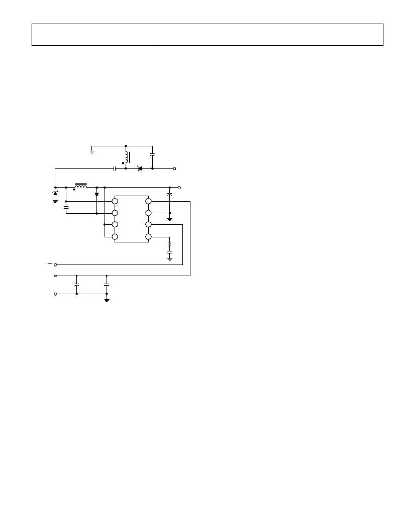
�Dual� Output� SEPIC� Regulator�
�For� many� systems,� a� dual� polarity� supply� is� needed.� The� circuit�
�in� Figure� 30� generates� both� a� positive� and� a� negative� 5� V� output�
�using� a� single� magnetic� component.� The� two� inductors� shown�
�are� actually� two� separate� windings� on� a� single� core� contained� in� a�
�small,� surface-mount� package.� The� windings� can� be� connected� in�
�parallel� or� in� series� to� be� used� as� a� single� inductor� for� a� conven-�
�tional� buck� regulator,� or� they� can� be� used� as� a� 1:1� transformer,�
�as� in� this� application.� The� first� winding� is� used� as� the� standard�
�buck� inductor� for� the� +5� V� output.� The� second� winding� is� used�
�to� generate� the� ?5� V� output� along� with� D2,� C6,� and� C7.�
�ADP3050�
�connected� to� produce� the� ?5� V� supply.� The� ?5� V� output� is�
�generated� even� without� C6� in� the� circuit,� but� its� inclusion�
�greatly� improves� the� regulation� of� the� negative� output� and�
�lowers� the� inductor� ripple� current.� The� total� output� current�
�available� for� both� supplies� is� limited� by� the� ADP3050� (internally�
�limited� to� around� 1.0� A).�
�Keeping� load� currents� below� 500� mA� and� 250� mA,� for� the�
�positive� and� negative� supplies,� respectively,� ensures� that� the�
�current� limit� is� not� reached� under� normal� operation.� These�
�limits� are� not� interchangeable;� 500� mA� cannot� be� drawn� from�
�the� ?5� V� supply� while� drawing� only� 250� mA� from� the� +5� V�
�D1�
�1N5818�
�C3�
�L1*�
�25μH�
�D3�
�1N4148�
�L1*�
�25μH�
�+�
�C6� D2�
�100μF� 1N5818�
�1� SWITCH� IN� 8�
�+� C7�
�100μF�
�–5V� AT� 0.25A�
�V� OUT�
�+5V� AT� 0.5A�
�V� OUT�
�+� C5�
�100μF�
�supply.� The� maximum� current� available� from� the� ?5� V� output� is�
�directly� related� to� the� +5� V� load� current,� due� to� the� fact� that� the�
�+5� V� output� is� used� to� regulate� both� supplies.� Typically,� the� ?5� V�
�load� current� should� be� around� one-half� of� the� +5� V� load� current�
�to� ensure� good� regulation� of� both� outputs.� Additionally,� the� ?5� V�
�output� should� have� a� preload� (the� minimum� current� level)� of�
�1%� to� 2%� of� the� +5� V� load� current.� This� helps� maintain� good�
�regulation� of� the� ?5� V� output� at� light� loads.�
�0.22μF�
�2� BOOST�
�3� BIAS�
�GND� 7�
�SD� 6�
�The� ripple� voltage� of� the� +5� V� output� is� that� of� a� normal� buck�
�regulator� as� described� in� the� Applications� Information� section.�
�This� ripple� voltage� is� determined� by� the� inductor� ripple� current�
�*INDUCTOR� IS� A� SINGLE� CORE�
�WITH� TWO� WINDINGS�
�COILTRONICS� CTX25-4�
�SD�
�12V�
�V� IN�
�+� C1�
�22μF�
�GND�
�4� FB� COMP� 5�
�U1�
�ADP3050-5�
�C2�
�0.01μF�
�R1�
�5.1k?�
�C4�
�1nF�
�and� the� ESR� of� the� output� capacitor.� For� Figure� 30,� the� positive�
�output� voltage� ripple� is� a� 30� mV� peak-to-peak� triangular� wave.�
�The� ripple� voltage� of� the� ?5� V� output� is� a� rectangular� wave,� due�
�to� the� rectangular� shape� of� the� current� waveform� into� the� ?5� V�
�output� capacitor.� The� amplitude� of� this� current� waveform� is�
�approximately� equal� to� twice� the� ?5� V� load� current.� For� a� load�
�current� of� 200� mA� and� an� ESR� of� 100� mΩ,� the� negative� output�
�voltage� ripple� is� approximately� 2� ×� 200� mA� ×� 100� mΩ,� or� about�
�Figure� 30.� Dual� Output� +5� V� and� ?5� V� Regulator�
�These� components� form� a� single-ended� primary� inductance�
�converter� (SEPIC)� using� the� 1:1� coupled� inductor� to� generate�
�the� negative� supply.� When� the� switch� is� off,� the� voltage� across�
�the� buck� winding� is� equal� to� V� O� +� V� D� (V� D� is� the� diode� drop).�
�This� voltage� is� generated� across� the� second� winding,� which� is�
�40� mV.� The� edges� of� this� ripple� waveform� are� quite� fast.� Along�
�with� the� inductance� of� the� output� capacitor,� it� generates� narrow�
�spikes� on� the� negative� output� voltage.� These� spikes� can� easily� be�
�filtered� out� using� an� additional� 5� μF� to� 10� μF� bypass� capacitor�
�close� to� the� load� (the� inductance� of� the� PCB� trace� and� the�
�additional� capacitor� create� a� low-pass� filter� to� remove� these�
�high� frequency� spikes).�
�Rev.� C� |� Page� 19� of� 20�
�相关PDF资料 |
PDF描述 |
|---|---|
| CT8BK40-M | 8" BLACK 40LB CABLE TIE |
| RLF12560T-100M7R5 | INDUCTOR PWR 10UH 20% 12560 SMD |
| M7KKK-3610J | IDC CABLE - MDG36K/MC37G/MDG36K |
| A9CAA-0606E | FLEX CABLE - AFK06A/AE06/AFH06T |
| ISL21007BFB825Z-TK | IC VREF SERIES PREC 2.5V 8-SOIC |
相关代理商/技术参数 |
参数描述 |
|---|---|
| ADP3050-EVALZ | 制造商:AD 制造商全称:Analog Devices 功能描述:200 kHz, 1 A High Voltage Step-Down Switching Regulator |
| ADP3051 | 制造商:AD 制造商全称:Analog Devices 功能描述:500 mA PWM Step-Down DC-DC with Synchronous Rectifier |
| ADP3051ARMZ-REEL | 制造商:Analog Devices 功能描述:CONV DC-DC SGL-OUT STEP DOWN 8MSOP - Tape and Reel |
| ADP3051ARMZ-REEL7 | 制造商:Analog Devices 功能描述:Conv DC-DC Single Step Down 2.7V to 5.5V 8-Pin MSOP T/R 制造商:Analog Devices 功能描述:SWITCH REG SYNC BUCK 500MA 8MSOP |
| ADP3088 | 制造商:AD 制造商全称:Analog Devices 功能描述:1 MHz, 750 mA Buck Regulator |
发布紧急采购,3分钟左右您将得到回复。