- 您现在的位置:买卖IC网 > PDF目录13176 > ADP322ACPZ-135-R7 (Analog Devices Inc)IC REG LDO 3.3/2.5/1.8V 16LFCSP PDF资料下载
参数资料
| 型号: | ADP322ACPZ-135-R7 |
| 厂商: | Analog Devices Inc |
| 文件页数: | 17/24页 |
| 文件大小: | 0K |
| 描述: | IC REG LDO 3.3/2.5/1.8V 16LFCSP |
| 标准包装: | 1 |
| 稳压器拓扑结构: | 正,固定式 |
| 输出电压: | 3.3V,2.5V,1.8V |
| 输入电压: | 1.8 V ~ 5.5 V |
| 电压 - 压降(标准): | 0.11V @ 200mA,0.11V @ 200mA,- |
| 稳压器数量: | 3 |
| 电流 - 输出: | 200mA(最小值) |
| 电流 - 限制(最小): | 250mA |
| 工作温度: | -40°C ~ 125°C |
| 安装类型: | 表面贴装 |
| 封装/外壳: | 16-WFQFN 裸露焊盘,CSP |
| 供应商设备封装: | 16-LFCSP-WQ(3x3) |
| 包装: | 标准包装 |
| 其它名称: | ADP322ACPZ-135-R7DKR |
�� �
�
�Data� Sheet�
�Use� Equation� 1� to� determine� the� worst-case� capacitance,�
�accounting� for� capacitor� variation� over� temperature,� compo-�
�nent� tolerance,� and� voltage.�
�ADP322/ADP323�
�As� shown� in� Figure� 48,� the� ENx� pin� has� built-in� hysteresis.� This�
�prevents� on/off� oscillations� that� can� occur� due� to� noise� on� the�
�ENx� pin� as� it� passes� through� the� threshold� points.�
�C� EFF� =� C� BIAS� � (1� ?� TEMPCO� )� � (1� ?� TOL� )�
�where:�
�C� BIAS� is� the� effective� capacitance� at� the� operating� voltage.�
�TEMPCO� is� the� worst-case� capacitor� temperature� coefficient.�
�TOL� is� the� worst-case� component� tolerance.�
�In� this� example,� TEMPCO� over� ?40°C� to� +85°C� is� assumed�
�to� be� 15%� for� an� X5R� dielectric.� TOL� is� assumed� to� be� 10%,�
�and� C� BIAS� is� 0.94� μF� at� 1.8� V� (from� the� graph� in� Figure� 47).�
�Substituting� these� values� into� Equation� 1� yields�
�(1)�
�The� active/inactive� thresholds� of� the� ENx� pin� are� derived�
�from� the� V� BIAS� voltage.� Therefore,� these� thresholds� vary� with�
�changing� input� voltage.� Figure� 49� shows� typical� ENx� active/�
�inactive� thresholds� when� the� input� voltage� varies� from� 2.5� V�
�to� 5.5� V� (note� that� V� ENx� is� the� enable� voltage).�
�1.00�
�0.95�
�0.90�
�0.85�
�C� EFF� =� 0.94� μF� ×� (1� ?� 0.15)� ×� (1� ?� 0.1)� =� 0.719� μF�
�Therefore,� the� capacitor� chosen� in� this� example� meets� the� mini-�
�mum� capacitance� requirement� of� the� LDO� over� temperature�
�and� tolerance� at� the� chosen� output� voltage.�
�To� guarantee� the� performance� of� the� ADP322/ADP323� triple�
�LDO,� it� is� imperative� that� the� effects� of� dc� bias,� temperature,�
�0.80�
�0.75�
�0.70�
�0.65�
�0.60�
�0.55�
�V� ENx� RISE�
�V� ENx� FALL�
�and� tolerances� on� the� behavior� of� the� capacitors� be� evaluated�
�0.50�
�2.5�
�3.0�
�3.5�
�4.0�
�4.5�
�5.0�
�5.5�
�for� each� application.�
�UNDERVOLTAGE� LOCKOUT�
�The� ADP322/ADP323� have� an� internal� undervoltage� lockout�
�circuit� that� disables� all� inputs� and� the� output� when� the� input�
�voltage� bias,� VBIAS,� is� less� than� approximately� 2.2� V.� This�
�ensures� that� the� inputs� of� the� ADP322/ADP323� and� the� output�
�behave� in� a� predictable� manner� during� power-up.�
�ENABLE� FEATURE�
�The� ADP322/ADP323� use� the� ENx� pins� to� enable� and� disable�
�INPUT� VOLTAGE� (V)�
�Figure� 49.� Typical� ENx� Pins� Thresholds� vs.� Input� Voltage�
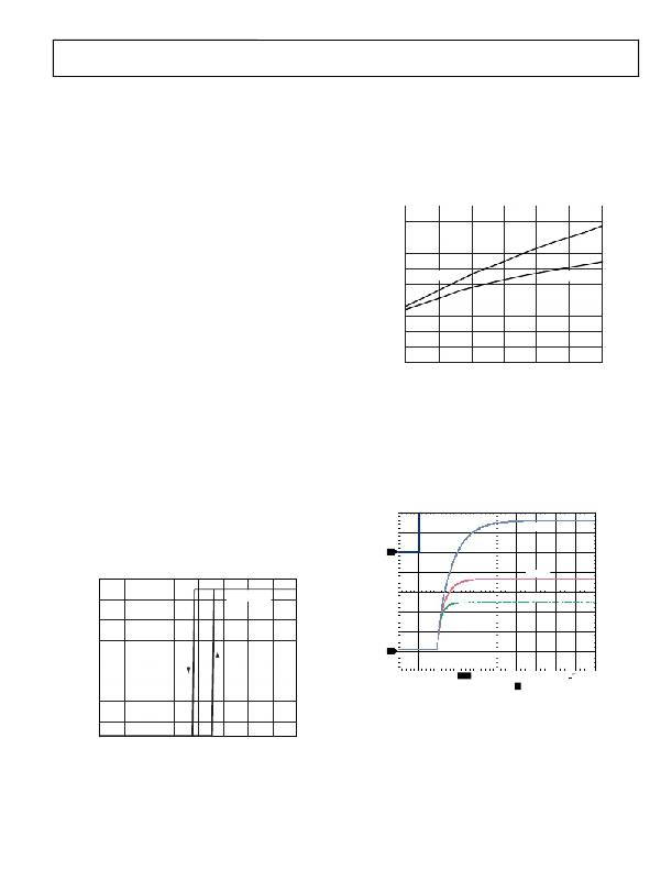
�The� ADP322/ADP323� use� an� internal� soft� start� to� limit� the�
�inrush� current� when� the� output� is� enabled.� The� start-up� time�
�for� the� 2.8� V� option� is� approximately� 220� μs� from� the� time� the�
�ENx� active� threshold� is� crossed� to� when� the� output� reaches� 90%�
�of� its� final� value.� The� start-up� time� is� somewhat� dependent� on�
�the� output� voltage� setting� and� increases� slightly� as� the� output�
�voltage� increases.�
��shows� that,� when� a� rising� voltage� on� ENx� crosses� the� active�
�threshold,� VOUTx� turns� on.� When� a� falling� voltage� on� ENx�
�V� ENx�
�V� OUT1�
�crosses� the� inactive� threshold,� VOUTx� turns� off.�
�1.4�
�1�
�V� OUT2�
�1.2�
�V� OUT� @� 4.5V� IN�
�V� OUT3�
�1.0�
�0.8�
�2�
�0.6�
�W�
�W�
�W�
�W�
�0.4�
�CH1� 1V�
�CH3� 500mV�
�B�
�B�
�CH2� 500mV�
�CH4� 500mV�
�B�
�B�
�M100μs� A� CH1�
�T� 10.2%�
�540mV�
�0.2�
�Figure� 50.� Typical� Start-Up� Time,I� LOAD1� =� I� LOAD2� =� I� LOAD3� =� 100� mA,�
�CH1� =� V� ENx� (the� Enable� Voltage),� CH2� =� V� OUT1� ,� CH3� =� V� OUT2� ,� CH4� =� V� OUT3�
�0�
�0.4�
�0.5�
�0.6�
�0.7�
�0.8�
�0.9�
�1.0�
�1.1�
�1.2�
�ENABLE� VOLTAGE� (V)�
�Figure� 48.� Typical� ENx� Pin� Operation�
�Rev.� A� |� Page� 17� of� 24�
�相关PDF资料 |
PDF描述 |
|---|---|
| 200TXW330MEFC16X40 | CAP ALUM 330UF 200V 20% RADIAL |
| GMM43DRUN | CONN EDGECARD 86POS DIP .156 SLD |
| VI-25D-EX-F1 | CONVERTER MOD DC/DC 85V 75W |
| VI-J6H-EW-S | CONVERTER MOD DC/DC 52V 100W |
| 400KXW150MEFC18X35 | CAP ALUM 150UF 400V 20% RADIAL |
相关代理商/技术参数 |
参数描述 |
|---|---|
| ADP322ACPZ-145 | 制造商:Analog Devices 功能描述:IC LDO TRIPLE 0.2A 16LFCSP 制造商:Analog Devices 功能描述:IC, LDO, TRIPLE, 0.2A, 16LFCSP 制造商:Analog Devices 功能描述:IC, LDO, TRIPLE, 0.2A, 16LFCSP; Primary Input Voltage:3.8V; Output Voltage Fixed:3.3V; Dropout Voltage Vdo:110mV; Voltage Regulator Case Style:LFCSP; No. of Pins:16; Output Current:200mA; Operating Temperature Min:-40C; Operating ;RoHS Compliant: Yes |
| ADP322ACPZ-145-R7 | 功能描述:IC REG LDO 3.3/2.5/1.2V 16LFCSP RoHS:是 类别:集成电路 (IC) >> PMIC - 稳压器 - 线性 系列:- 标准包装:45 系列:- 稳压器拓扑结构:正,固定式 输出电压:5V 输入电压:6 V ~ 30 V 电压 - 压降(标准):0.47V @ 250mA 稳压器数量:1 电流 - 输出:250mA 电流 - 限制(最小):- 工作温度:-40°C ~ 125°C 安装类型:通孔 封装/外壳:TO-220-3 供应商设备封装:TO-220-3 包装:管件 产品目录页面:1289 (CN2011-ZH PDF) 其它名称:*LP2954AIT*LP2954AIT/NOPBLP2954AIT |
| ADP322ACPZ-155 | 制造商:Analog Devices 功能描述:IC LDO TRIPLE 0.2A 16LFCSP 制造商:Analog Devices 功能描述:IC, LDO, TRIPLE, 0.2A, 16LFCSP |
| ADP322ACPZ-155-R7 | 功能描述:IC REG LDO 3.3/1.8/1.5V 16LFCSP RoHS:是 类别:集成电路 (IC) >> PMIC - 稳压器 - 线性 系列:- 标准包装:75 系列:- 稳压器拓扑结构:正,可调式 输出电压:1.2 V ~ 37 V 输入电压:4.2 V ~ 40 V 电压 - 压降(标准):- 稳压器数量:1 电流 - 输出:500mA 电流 - 限制(最小):500mA 工作温度:-40°C ~ 125°C 安装类型:表面贴装 封装/外壳:TO-252-3,DPak(2 引线+接片),SC-63 供应商设备封装:TO-252-3 包装:管件 产品目录页面:1286 (CN2011-ZH PDF) 其它名称:*LM317AMDT/NOPBLM317AMDT |
| ADP322ACPZ-165-R7 | 功能描述:IC REG LDO 3.3/1.8/1.2V 16LFCSP RoHS:是 类别:集成电路 (IC) >> PMIC - 稳压器 - 线性 系列:- 标准包装:45 系列:- 稳压器拓扑结构:正,固定式 输出电压:5V 输入电压:6 V ~ 30 V 电压 - 压降(标准):0.47V @ 250mA 稳压器数量:1 电流 - 输出:250mA 电流 - 限制(最小):- 工作温度:-40°C ~ 125°C 安装类型:通孔 封装/外壳:TO-220-3 供应商设备封装:TO-220-3 包装:管件 产品目录页面:1289 (CN2011-ZH PDF) 其它名称:*LP2954AIT*LP2954AIT/NOPBLP2954AIT |
发布紧急采购,3分钟左右您将得到回复。