- 您现在的位置:买卖IC网 > PDF目录4781 > ADP322ACPZ-145-R7 (Analog Devices Inc)IC REG LDO 3.3/2.5/1.2V 16LFCSP PDF资料下载
参数资料
| 型号: | ADP322ACPZ-145-R7 |
| 厂商: | Analog Devices Inc |
| 文件页数: | 15/24页 |
| 文件大小: | 0K |
| 描述: | IC REG LDO 3.3/2.5/1.2V 16LFCSP |
| 标准包装: | 1 |
| 稳压器拓扑结构: | 正,固定式 |
| 输出电压: | 3.3V,2.5V,1.2V |
| 输入电压: | 1.8 V ~ 5.5 V |
| 电压 - 压降(标准): | 0.11V @ 200mA,0.11V @ 200mA,- |
| 稳压器数量: | 3 |
| 电流 - 输出: | 200mA(最小值) |
| 电流 - 限制(最小): | 250mA |
| 工作温度: | -40°C ~ 125°C |
| 安装类型: | 表面贴装 |
| 封装/外壳: | 16-WFQFN 裸露焊盘,CSP |
| 供应商设备封装: | 16-LFCSP-WQ(3x3) |
| 包装: | 标准包装 |
| 其它名称: | ADP322ACPZ-145-R7DKR |
�� ��
��
��Data� Sheet�
�THEORY� OF� OPERATION�
�The� ADP322/ADP323� triple� LDO� are� low� quiescent� current,� low�
�dropout� linear� regulators� that� operate� from� 1.8� V� to� 5.5� V� on�
�VIN1/VIN2� and� VIN3� and� provide� up� to� 200� mA� of� current� from�
�each� output.� Drawing� a� low� 250� μA� quiescent� current� (typical)� at�
�full� load� makes� the� ADP322/ADP323� ideal� for� battery-operated�
�portable� equipment.� Shutdown� current� consumption� is� typically�
�100� nA.� Optimized� for� use� with� small� 1� μF� ceramic� capacitors,�
�the� ADP322/ADP323� provide� excellent� transient� performance.�
�Internally,� the� ADP322� consists� of� a� reference,� three� error� ampli-�
�fiers,� three� feedback� voltage� dividers,� and� three� PMOS� pass�
�transistors.� Output� current� is� delivered� via� the� PMOS� pass� device,�
�which� is� controlled� by� the� error� amplifier.� The� error� amplifier�
�compares� the� reference� voltage� with� the� feedback� voltage� from� the�
�output� and� amplifies� the� difference.� If� the� feedback� voltage� is� lower�
�than� the� reference� voltage,� the� gate� of� the� PMOS� device� is� pulled�
�lower,� allowing� more� current� to� flow� and� increasing� the� output� vol-�
�tage.� If� the� feedback� voltage� is� higher� than� the� reference� voltage,� the�
�gate� of� the� PMOS� device� is� pulled� higher,� allowing� less� current�
�to� flow� and� decreasing� the� output� voltage.�
�ADP322/ADP323�
�The� output� voltage� can� be� set� using� the� following� formulas:�
�V� OUT� =� 0.5� V(1� +� R1� /� R2� )� +� (� FB� IN� )(� R1� )�
�V� OUT2� =� 0.5� V(1� +� R3� /� R4� )� +� (� FB� IN� )(� R3� )�
�V� OUT3� =� 0.5� V(1� +� R5/� R6� )� +� (� FB� IN� )(� R5� )�
�The� value� of� R1,� R3,� R5� should� be� less� than� 200� k� to� minimize�
�errors� in� the� output� voltage� caused� by� the� FBx� pin� input�
�current.� For� example,� when� R1� and� R2� each� equal� 200� kΩ,� the�
�output� voltage� is� 1.0� V.� The� output� voltage� error� introduced� by�
�the� FBx� pin� input� current� is� 2� mV� or� 0.20%,� assuming� a� typical�
�FBx� pin� input� current� of� 10� nA� at� 25°C.�
�The� ADP322� is� available� in� multiple� output� voltage� options�
�ranging� from� 0.8� V� to� 3.3� V.�
�The� ADP322/ADP323� use� the� EN1/EN2� and� EN3� pins� to�
�enable� and� disable� the� VOUT1/VOUT2/VOUT3� pins� under�
�normal� operating� conditions.� When� the� EN1/EN2� and� EN3�
�pins� are� high,� VOUT1/VOUT2/VOUT3� turn� on;� when� the�
�EN1/EN2� and� EN3� pins� are� low,� VOUT1/VOUT2/VOUT3� turn�
�VIN1/VIN2�
�VOUT1�
�off.� For� automatic� startup,� the� EN1/EN2� and� EN3� pins� can� be�
�tied� to� VBIAS.�
�VBIAS�
�EN1�
�INTERNAL� BIAS�
�VOLTAGES/CURRENTS,�
�UVLO� AND� THERMAL�
�PROTECT�
�SHUTDOWN�
�VOUT1�
�OVERCURRENT�
�+�
�–�
�0.5V�
�REF�
�VOUT2�
�2.5V� TO�
�5.5V�
�+�
�1μF�
�VBIAS�
�ADP323�
�VBIAS�
�1μF�
�EN1�
�EN2�
�EN3�
�SHUTDOWN�
�VOUT2�
�SHUTDOWN�
�VOUT3�
�OVERCURRENT�
�+�
�–�
�0.5V�
�REF�
�1.8V� TO�
�5.5V�
�+�
�VIN1/VIN2�
�ON�
�OFF�
�LDO� 1�
�EN� LD1�
�FB1�
�R1�
�VOUT1�
�+�
�1μF�
�VIN3�
�VOUT3�
�VBIAS�
�R2�
�VOUT2�
�GND�
�OVERCURRENT�
�+�
�–�
�EN2�
�OFF�
�ON�
�LDO� 2�
�EN� LD2�
�FB2�
�R3�
�+�
�1μF�
�0.5V�
�REF�
�VBIAS�
�R4�
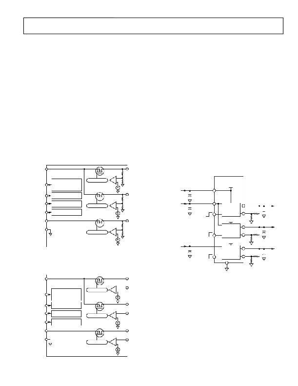
�Figure� 43.� ADP322� Internal� Block� Diagram�
�The� ADP323� differs� from� the� ADP322� except� in� that� the� output�
�voltage� dividers� are� internally� disconnected� and� the� feedback�
�1.8V� TO�
�5.5V�
�+�
�1μF�
�EN3�
�VIN3�
�ON�
�OFF�
�LDO� 3�
�EN� LD3�
�GND�
�FB3�
�R5�
�R6�
�VOUT3�
�+�
�1μF�
�inputs� of� the� error� amplifiers� are� brought� out� for� each� output.�
�Figure� 45.� ADP323� Application� Circuit� Diagram�
�VIN1/VIN2�
�VOUT1�
�VBIAS�
�EN1�
�EN2�
�EN3�
�INTERNAL� BIAS�
�VOLTAGES/CURRENTS,�
�UVLO� AND� THERMAL�
�PROTECT�
�SHUTDOWN�
�VOUT1�
�SHUTDOWN�
�VOUT2�
�SHUTDOWN�
�VOUT3�
�OVERCURRENT�
�OVERCURRENT�
�+�
�–�
�0.5V�
�REF�
�+�
�–�
�0.5V�
�REF�
�FB1�
�VOUT2�
�FB2�
�VIN3�
�VOUT3�
�GND�
�OVERCURRENT�
�+�
�–�
�FB3�
�0.5V�
�REF�
�Figure� 44.� ADP323� Internal� Block� Diagram�
�Rev.� A� |� Page� 15� of� 24�
�相关PDF资料 |
PDF描述 |
|---|---|
| MIC5305-4.75YD5 TR | IC REG LDO 4.75V .15A TSOT23-5 |
| MIC5305-2.7YD5 TR | IC REG LDO 2.7V .15A TSOT23-5 |
| MIC5206YMM TR | IC REG LDO ADJ .15A 8-MSOP |
| GCB85DHLD | CONN EDGECARD 170PS .050 DIP SLD |
| EYM36DRMT-S664 | CONN EDGECARD 72POS .156 WW |
相关代理商/技术参数 |
参数描述 |
|---|---|
| ADP322ACPZ-155 | 制造商:Analog Devices 功能描述:IC LDO TRIPLE 0.2A 16LFCSP 制造商:Analog Devices 功能描述:IC, LDO, TRIPLE, 0.2A, 16LFCSP |
| ADP322ACPZ-155-R7 | 功能描述:IC REG LDO 3.3/1.8/1.5V 16LFCSP RoHS:是 类别:集成电路 (IC) >> PMIC - 稳压器 - 线性 系列:- 标准包装:75 系列:- 稳压器拓扑结构:正,可调式 输出电压:1.2 V ~ 37 V 输入电压:4.2 V ~ 40 V 电压 - 压降(标准):- 稳压器数量:1 电流 - 输出:500mA 电流 - 限制(最小):500mA 工作温度:-40°C ~ 125°C 安装类型:表面贴装 封装/外壳:TO-252-3,DPak(2 引线+接片),SC-63 供应商设备封装:TO-252-3 包装:管件 产品目录页面:1286 (CN2011-ZH PDF) 其它名称:*LM317AMDT/NOPBLM317AMDT |
| ADP322ACPZ-165-R7 | 功能描述:IC REG LDO 3.3/1.8/1.2V 16LFCSP RoHS:是 类别:集成电路 (IC) >> PMIC - 稳压器 - 线性 系列:- 标准包装:45 系列:- 稳压器拓扑结构:正,固定式 输出电压:5V 输入电压:6 V ~ 30 V 电压 - 压降(标准):0.47V @ 250mA 稳压器数量:1 电流 - 输出:250mA 电流 - 限制(最小):- 工作温度:-40°C ~ 125°C 安装类型:通孔 封装/外壳:TO-220-3 供应商设备封装:TO-220-3 包装:管件 产品目录页面:1289 (CN2011-ZH PDF) 其它名称:*LP2954AIT*LP2954AIT/NOPBLP2954AIT |
| ADP322ACPZ-175-R7 | 功能描述:IC REG LDO 2.8/1.8/1.2V 16LFCSP RoHS:是 类别:集成电路 (IC) >> PMIC - 稳压器 - 线性 系列:- 标准包装:75 系列:- 稳压器拓扑结构:正,可调式 输出电压:1.2 V ~ 37 V 输入电压:4.2 V ~ 40 V 电压 - 压降(标准):- 稳压器数量:1 电流 - 输出:500mA 电流 - 限制(最小):500mA 工作温度:-40°C ~ 125°C 安装类型:表面贴装 封装/外壳:TO-252-3,DPak(2 引线+接片),SC-63 供应商设备封装:TO-252-3 包装:管件 产品目录页面:1286 (CN2011-ZH PDF) 其它名称:*LM317AMDT/NOPBLM317AMDT |
| ADP322ACPZ-189-R7 | 功能描述:IC REG LDO 2.5/1.8/1.2V 16LFCSP RoHS:是 类别:集成电路 (IC) >> PMIC - 稳压器 - 线性 系列:- 标准包装:45 系列:- 稳压器拓扑结构:正,固定式 输出电压:5V 输入电压:6 V ~ 30 V 电压 - 压降(标准):0.47V @ 250mA 稳压器数量:1 电流 - 输出:250mA 电流 - 限制(最小):- 工作温度:-40°C ~ 125°C 安装类型:通孔 封装/外壳:TO-220-3 供应商设备封装:TO-220-3 包装:管件 产品目录页面:1289 (CN2011-ZH PDF) 其它名称:*LP2954AIT*LP2954AIT/NOPBLP2954AIT |
发布紧急采购,3分钟左右您将得到回复。