参数资料
| 型号: | ADP3367ARZ |
| 厂商: | Analog Devices Inc |
| 文件页数: | 3/8页 |
| 文件大小: | 0K |
| 描述: | IC REG LDO 5V/ADJ .2A 8SOIC |
| 标准包装: | 98 |
| 稳压器拓扑结构: | 正,固定式或可调式 |
| 输出电压: | 5V,1.3 V ~ 16 V |
| 输入电压: | 2.5 V ~ 16.5 V |
| 电压 - 压降(标准): | 0.3V @ 300mA |
| 稳压器数量: | 1 |
| 电流 - 输出: | 200mA(最小值) |
| 工作温度: | -40°C ~ 85°C |
| 安装类型: | 表面贴装 |
| 封装/外壳: | 8-SOIC(0.154",3.90mm 宽) |
| 供应商设备封装: | 8-SOIC |
| 包装: | 管件 |
| 产品目录页面: | 795 (CN2011-ZH PDF) |
�� ������
������ADP3367�
�PIN� FUNCTION� DESCRIPTION�
�Mnemonic� Function�
�GENERAL� INFORMATION�
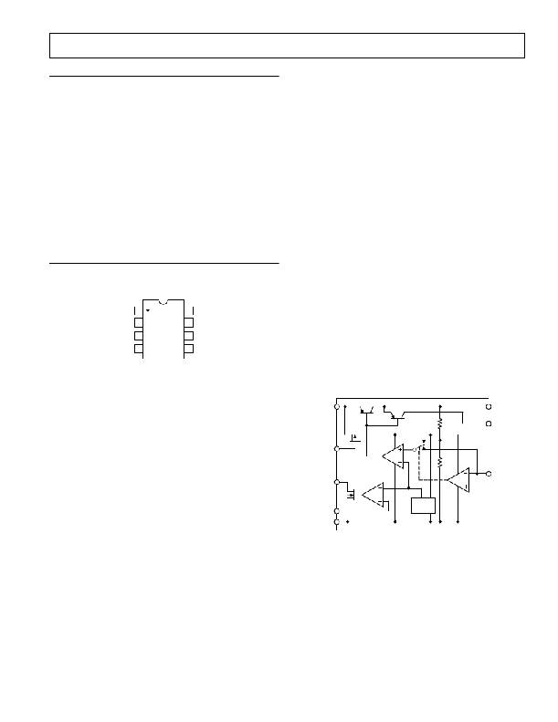
�The� ADP3367� contains� a� micropower� bandgap� reference� volt-�
�age� source,� an� error� amplifier� A1,� two� comparators� (C1,� C2)�
�DD�
�V� IN�
�GND�
�LBI�
�LBO�
�SHDN�
�SET�
�OUT�
�Dropout� Detector� Output.� PNP� collector� output�
�which� sources� current� as� dropout� is� reached.�
�Voltage� Regulator� Input.�
�Ground� Pin.� Must� be� connected� to� 0� V.�
�Low� Battery� Detect� Input.� Compared� with� 1.255� V.�
�Low� Battery� Detect� Output.� Open� Drain� Output�
�that� goes� low� when� LBI� is� below� the� threshold.�
�Digital� Input.� May� be� used� to� disable� the� device�
�so� that� the� power� consumption� is� minimized.�
�Voltage� Setting� Input.� Connect� to� GND� for� +5� V�
�output� or� connect� to� resistive� divider� for� adjust-�
�able� output.�
�Regulated� Output� Voltage.� Connect� to� filter�
�capacitor.�
�DIP� &� SOIC� PIN� CONFIGURATION�
�and� a� series� PNP� output� pass� transistor.�
�CIRCUIT� DESCRIPTION�
�The� internal� bandgap� voltage� reference� is� trimmed� to� 1.255� V�
�and� is� used� as� a� reference� input� to� the� error� amplifier� A1.� The�
�feedback� signal� from� the� regulator� output� is� supplied� to� the�
�other� input� by� an� on-chip� voltage� divider� or� by� two� external�
�resistors.� When� the� SET� input� is� at� ground,� the� internal� divider�
�provides� the� error� amplifier’s� feedback� signal� giving� a� +5� V� out-�
�put.� When� SET� is� at� more� than� 50� mV� above� ground,� compara-�
�tor� C1� switches� the� error� amplifier’s� input� directly� to� the� SET�
�pin,� and� external� resistors� are� used� to� set� the� output� voltage.�
�The� external� resistors� are� selected� so� that� the� desired� output�
�voltage� gives� 1.255� V� at� the� SET� input.�
�The� output� from� the� error� amplifier� supplies� base� current� to� the�
�PNP� output� pass� transistor� which� provides� output� current.� Up�
�to� 300� mA� output� current� is� available� provided� that� the� device�
�power� dissipation� is� not� exceeded.�
�Comparator� C2� compares� the� voltage� on� the� Low� Battery� Input�
�(LBI)� pin� to� the� internal� +1.255� V� reference� voltage.� The� out-�
�DD�
�1�
�8�
�IN�
�put� from� the� comparator� drives� an� open� drain� FET� connected�
�OUT�
�LBI�
�GND�
�2�
�3�
�4�
�ADP3367�
�TOP� VIEW�
�(Not� to� Scale)�
�7�
�6�
�5�
�LBO�
�SET�
�SHDN�
�to� the� Low� Battery� Output� pin,� LBO.� The� Low� Battery� Thresh-�
�old� may� be� set� using� a� suitable� voltage� divider� connected� to�
�LBI.� When� the� voltage� on� LBI� falls� below� 1.255� V,� the� open�
�drain� output,� LBO,� is� pulled� low.�
�A� shutdown� (SHDN)� input� that� can� be� used� to� disable� the�
�TERMINOLOGY�
�Dropout� Voltage:� The� input/output� voltage� differential� at�
�error� amplifier� and� hence� the� voltage� output� is� also� available.�
�The� supply� current� in� shutdown� is� less� than� 0.75� μ� A.�
�which� the� regulator� no� longer� maintains� regulation� against� fur-�
�ther� reductions� in� input� voltage.� It� is� measured� when� the� output�
�decreases� 100� mV� from� its� nominal� value.� The� nominal� value� is�
�the� measured� value� with� V� IN� =� V� OUT� +2� V.�
�IN�
�ADP3367�
�OUT�
�DD�
�Line� Regulation� :� The� change� in� output� voltage� as� a� result� of� a�
�change� in� the� input� voltage.� It� is� specified� for� a� change� of� input�
�voltage� from� 6� V� to� 10� V.�
�SHDN�
�A1�
�SET�
�Load� Regulation:� The� change� in� output� voltage� for� a� change�
�in� output� current.� It� is� specified� for� an� output� current� change�
�LBO�
�C2�
�C1�
�from� 10� mA� to� 200� mA.�
�Quiescent� Current� (I� GND� ):� The� input� bias� current� which�
�flows� into� the� regulator� not� including� load� current.� It� is� mea-�
�LBI�
�GND�
�1.255V�
�REF�
�50mV�
�sured� on� the� GND� line� and� is� specified� in� shutdown� and� also� for�
�different� values� of� load� current.�
�Shutdown:� The� regulator� is� disabled� and� power� consumption�
�is� minimized.�
�Dropout� Detector:� An� output� that� indicates� that� the� regulator�
�is� dropping� out� of� regulation.�
�Maximum� Power� Dissipation:� The� maximum� total� device�
�dissipation� for� which� the� regulator� will� continue� to� operate�
�within� specifications.�
�REV.� A� 0�
�–3� –�
�Figure� 1.� ADP3367� Functional� Block� Diagram�
�相关PDF资料 |
PDF描述 |
|---|---|
| 400VXR220MEFCSN25X45 | CAP ALUM 220UF 400V 20% SNAP-IN |
| ASPI-0704S-220M | INDUCTOR POWER 22UH 0704 SMD |
| ABM15DTKN-S288 | CONN EDGECARD EXTEND 30POS .156 |
| LT3021ES8-1.5#PBF | IC REG LDO 1.5V .5A 8-SOIC |
| ASPI-0704S-180M | INDUCTOR POWER 18UH 0704 SMD |
相关代理商/技术参数 |
参数描述 |
|---|---|
| ADP3367ARZ | 制造商:Analog Devices 功能描述:LDO 2.5-16.5V 0.3VDO 0.3A 8SOIC |
| ADP3367ARZ-REEL | 制造商:Analog Devices 功能描述:LDO Regulator Pos 1.3V to 16V5V 0.2A 8-Pin SOIC N T/R |
| ADP3367ARZ-REEL7 | 功能描述:IC REG LDO 5V/ADJ .2A 8SOIC RoHS:是 类别:集成电路 (IC) >> PMIC - 稳压器 - 线性 系列:- 标准包装:800 系列:- 稳压器拓扑结构:正,固定式 输出电压:2.5V 输入电压:最高 16V 电压 - 压降(标准):0.7V @ 4A 稳压器数量:1 电流 - 输出:4A 电流 - 限制(最小):4.2A 工作温度:0°C ~ 125°C 安装类型:表面贴装 封装/外壳:TO-263-6,D²Pak(5 引线+接片),TO-263BA 供应商设备封装:TO-263-5 包装:带卷 (TR) 其它名称:AP1184K525L-13AP1184K525LDITR |
| ADP3401 | 制造商:AD 制造商全称:Analog Devices 功能描述:GSM Power Management System |
| ADP3401ARU | 制造商:AD 制造商全称:Analog Devices 功能描述:GSM Power Management System |
发布紧急采购,3分钟左右您将得到回复。