- 您现在的位置:买卖IC网 > PDF目录294846 > ADP3629ARZ-R7 (ANALOG DEVICES INC) High Speed, Dual, 2 A MOSFET Driver, inverting A/B input pins; Package: 8 ld SOIC; No of Pins: 8; Temperature Range: Ind PDF资料下载
参数资料
| 型号: | ADP3629ARZ-R7 |
| 厂商: | ANALOG DEVICES INC |
| 元件分类: | MOSFETs |
| 英文描述: | High Speed, Dual, 2 A MOSFET Driver, inverting A/B input pins; Package: 8 ld SOIC; No of Pins: 8; Temperature Range: Ind |
| 中文描述: | 2 A 2 CHANNEL, BUF OR INV BASED MOSFET DRIVER, PDSO8 |
| 封装: | ROHS COMPLIANT, MS-012-AA, SOIC-8 |
| 文件页数: | 3/16页 |
| 文件大小: | 361K |
| 代理商: | ADP3629ARZ-R7 |
ADP3629/ADP3630/ADP3631
Rev. 0 | Page 11 of 16
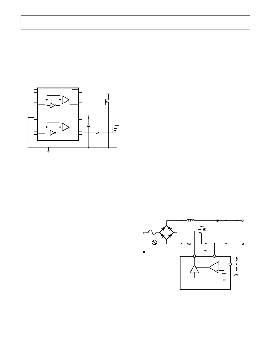
THEORY OF OPERATION
The ADP3629/ADP3630/ADP3631 family of dual drivers is
optimized for driving two independent enhancement N-channel
MOSFETs or insulated gate bipolar transistors (IGBTs) in high
switching frequency applications.
These applications require high speed, fast rise and fall times, and
short propagation delays. The capacitive nature of MOSFETs and
IGBTs requires high peak current capability, as well.
VDD
VDD
PGND
OUTA
OUTB
SD
OTW
1
3
8
7
6
5
2
4
VDS
ADP3629/ADP3630/ADP3631
B
NONINVERTING
INVERTING
A
NONINVERTING
INVERTING
INA,
INA
INB,
INB
08
40
1-
01
7
Figure 21. Typical Application Circuit
INPUT DRIVE REQUIREMENTS (INA, INA, INB, INB,
AND SD)
The inputs of the ADP3629/ADP3630/ADP3631 are designed
to meet the requirements of modern digital power controllers;
the signals are compatible with 3.3 V logic levels. At the same
time, the input structure allows for input voltages as high as VDD.
The signals applied to the inputs (INA, INA, INB, and INB)
should have steep and clean fronts. It is not recommended that
slow changing signals be applied to drive these inputs because
such signals can result in multiple switching output signals
when the thresholds are crossed, causing damage to the power
MOSFET or IGBT.
An internal pull-down resistor is present at the input, which
guarantees that the power device is off in the event that the
input is left floating.
The SD input has a precision comparator with hysteresis and is
therefore suitable for slow changing signals (such as a scaled-
down output voltage); see the Shutdown (SD) Function section
for more information about this comparator.
LOW-SIDE DRIVERS (OUTA, OUTB)
The ADP3629/ADP3630/ADP3631 family of dual drivers is
designed to drive ground referenced N-channel MOSFETs. The
bias is internally connected to the VDD supply and to PGND.
When the ADP3629/ADP3630/ADP3631 are disabled, both
low-side gates are held low. An internal impedance is present
between the OUTA/OUTB pins and GND, even when VDD is
not present; this feature ensures that the power MOSFET is
normally off when bias voltage is not present.
When interfacing the ADP3629/ADP3630/ADP3631 to exter-
nal MOSFETs, the designer should consider ways to create a
robust design that minimizes stresses on both the driver and
the MOSFETs. These stresses include exceeding the short time
duration voltage ratings on the OUTA and OUTB pins, as well
as on the external MOSFET.
Power MOSFETs are usually selected to have low on resistance to
minimize conduction losses, which usually implies a large input
gate capacitance and gate charge.
SHUTDOWN (SD) FUNCTION
The ADP3629/ADP3630/ADP3631 feature an advanced shut-
down function with accurate thresholds and hysteresis.
The SD signal is an active high signal. An internal pull-up is
present on this pin and, therefore, it is necessary to pull down
the pin externally for the drivers to operate normally.
In some power systems, it is sometimes necessary to provide an
additional overvoltage protection (OVP) or overcurrent protection
(OCP) shutdown signal to turn off the power devices (MOSFETs
or IGBTs) in case of failure of the main controller.
An accurate internal reference is used for the SD comparator so
that it can be used to detect OVP or OCP fault conditions.
AC
INPUT
DC
OUTPUT
+
–
OUTA
PGND
VEN
SD
ADP3629/ADP3630/ADP3631
0
84
01
-0
18
Figure 22. Shutdown Function Used for Redundant OVP
相关PDF资料 |
PDF描述 |
|---|---|
| ADP3630ARMZ-R7 | High Speed, Dual, 2 A MOSFET Driver, non-inverting A/B input pins; Package: 8 ld MSOP; No of Pins: 8; Temperature Range: Ind |
| ADP3630ARZ-R7 | High Speed, Dual, 2 A MOSFET Driver, non-inverting A/B input pins; Package: 8 ld SOIC; No of Pins: 8; Temperature Range: Ind |
| ADP3631ARMZ-R7 | High Speed, Dual, 2 A MOSFET Driver, inverting A & non-inverting B input pins; Package: 8 ld MSOP; No of Pins: 8; Temperature Range: Ind |
| ADP3631ARZ-R7 | High Speed, Dual, 2 A MOSFET Driver, inverting A & non-inverting B input pins; Package: 8 ld SOIC; No of Pins: 8; Temperature Range: Ind |
| ADP3820ART-4.2-RL | 1-CHANNEL POWER SUPPLY SUPPORT CKT, PDSO6 |
相关代理商/技术参数 |
参数描述 |
|---|---|
| ADP3630 | 制造商:AD 制造商全称:Analog Devices 功能描述:High Speed, Dual, 2 A MOSFET Driver |
| ADP3630ARMZ-R7 | 功能描述:IC MOSFET DVR 2A DL HS 8MSOP RoHS:是 类别:集成电路 (IC) >> PMIC - MOSFET,电桥驱动器 - 外部开关 系列:- 标准包装:95 系列:- 配置:高端和低端,独立 输入类型:非反相 延迟时间:160ns 电流 - 峰:290mA 配置数:1 输出数:2 高端电压 - 最大(自引导启动):600V 电源电压:10 V ~ 20 V 工作温度:-40°C ~ 125°C 安装类型:表面贴装 封装/外壳:8-SOIC(0.154",3.90mm 宽) 供应商设备封装:8-SOIC 包装:管件 产品目录页面:1381 (CN2011-ZH PDF) |
| ADP3630ARZ-R7 | 功能描述:IC MOSFET DVR 2A DL HS 8SOIC RoHS:是 类别:集成电路 (IC) >> PMIC - MOSFET,电桥驱动器 - 外部开关 系列:- 标准包装:95 系列:- 配置:半桥 输入类型:PWM 延迟时间:25ns 电流 - 峰:1.6A 配置数:1 输出数:2 高端电压 - 最大(自引导启动):118V 电源电压:9 V ~ 14 V 工作温度:-40°C ~ 125°C 安装类型:表面贴装 封装/外壳:8-SOIC(0.154",3.90mm 宽) 供应商设备封装:8-SOIC 包装:管件 产品目录页面:1282 (CN2011-ZH PDF) 其它名称:*LM5104M*LM5104M/NOPBLM5104M |
| ADP3630ARZ-R7 | 制造商:Analog Devices 功能描述:Dual Non-Inverting MOSFET Driver IC |
| ADP3631 | 制造商:AD 制造商全称:Analog Devices 功能描述:High Speed, Dual, 2 A MOSFET Driver |
发布紧急采购,3分钟左右您将得到回复。