- 您现在的位置:买卖IC网 > PDF目录17000 > ADS8364EVM (Texas Instruments)EVALUATION MODULE FOR BQ2018 PDF资料下载
参数资料
| 型号: | ADS8364EVM |
| 厂商: | Texas Instruments |
| 文件页数: | 2/26页 |
| 文件大小: | 0K |
| 描述: | EVALUATION MODULE FOR BQ2018 |
| 产品培训模块: | Data Converter Basics |
| 标准包装: | 1 |
| ADC 的数量: | 6 |
| 位数: | 16 |
| 采样率(每秒): | 250k |
| 数据接口: | 并联 |
| 输入范围: | 0 ~ 5 V |
| 在以下条件下的电源(标准): | 413.5mW @ 250kSPS |
| 工作温度: | -40°C ~ 85°C |
| 已用 IC / 零件: | ADS8364 |
| 已供物品: | 板 |
| 相关产品: | 296-13449-6-ND - IC ADC LP 16BIT 250KSPS 64TQFP ADS8364Y/2KG4-ND - IC ADC LP 16BIT 250KSPS 64-TQFP ADS8364Y/2K-ND - IC ADC LP 16BIT 250KSPS 64-TQFP ADS8364Y/250G4-ND - IC ADC LP 16BIT 250KSPS 64-TQFP 296-13449-1-ND - IC ADC LP 16BIT 250KSPS 64TQFP 296-13449-2-ND - IC ADC LP 16BIT 250KSPS 64TQFP |
ADS8364
10
SBAS219C
www.ti.com
INTRODUCTION
The ADS8364 is a high-speed, low-power, 6-channel simul-
taneous sampling and converting, 16-bit ADC that operates
from a single +5V supply. The input channels are fully
differential with a typical common-mode rejection of 80dB.
The part contains six 4
s successive approximation ADCs,
six differential sample-and-hold amplifiers, an internal +2.5V
reference with REFIN and REFOUT pins and a high-speed
parallel interface. There are six analog inputs that are grouped
into three channel pairs (A, B, and C). There are six ADCs,
one for each input that can be sampled and converted
simultaneously, thus preserving the relative phase informa-
tion of the signals on both analog inputs. Each pair of
channels has a hold signal (HOLDA, HOLDB, and HOLDC)
to allow simultaneous sampling on each channel pair, on
four or on all six channels. The part accepts a differential
analog input voltage in the range of –VREF to +VREF, centered
on the common-mode voltage (see the Analog Input Section).
The part will also accept bipolar input ranges when a level shift
circuit is used at the front end (see Figure 6).
A conversion is initiated on the ADS8364 by bringing the
HOLDX pin LOW for a minimum of 20ns. HOLDX LOW
places the sample-and-hold amplifiers of the X channels in
the hold state simultaneously and the conversion process is
started on each channel. The EOC output will go LOW for
half a clock cycle when the conversion is latched into the
output register. The data can be read from the parallel output
bus following the conversion by bringing both RD and CS
LOW.
Conversion time for the ADS8364 is 3.2
s when a 5MHz
external clock is used. The corresponding acquisition time is
0.8
s. To achieve the maximum output data rate (250kSPS),
the read function can be performed during the next conver-
sion. Note: This mode of operation is described in more
detail in the Timing and Control section of this data sheet.
SAMPLE-AND-HOLD SECTION
The sample-and-hold amplifiers on the ADS8364 allow the
ADCs to accurately convert an input sine wave of full-scale
amplitude to 16-bit resolution. The input bandwidth of the
sample-and-hold is greater than the Nyquist rate (Nyquist
equals one-half of the sampling rate) of the ADC even when
the ADC is operated at its maximum throughput rate of
250kSPS. The typical small-signal bandwidth of the sample-
and-hold amplifiers is 300MHz.
Typical aperture delay time or the time it takes for the
ADS8364 to switch from the sample to the hold mode
following the negative edge of HOLDX signal is 5ns. The
average delta of repeated aperture delay values is typically
50ps (also known as aperture jitter). These specifications
reflect the ability of the ADS8364 to capture AC input signals
accurately at the exact same moment in time.
REFERENCE
Under normal operation, the REFOUT (pin 61) can directly be
connected to the REFIN pin (pin 62) to provide an internal
+2.5V reference to the ADS8364. The ADS8364 can
operate, however, with an external reference in the range of
1.5V to 2.6V, for a corresponding full-scale range of 3.0V to
5.2V, as long as the input does not exceed the AVDD + 0.3V
value.
The reference of the ADS8364 is double-buffered. If the
internal reference is used to drive an external load, a buffer
is provided between the reference and the load applied to pin
61 (the internal reference can typically source 10
A of
current—load capacitance should be 0.1
F and 10F to
minimize noise). If an external reference is used, the three-
second buffers provide isolation between the external refer-
ence and the CDACs. These buffers are also used to
recharge all of the capacitors of all CDACs during conver-
sion.
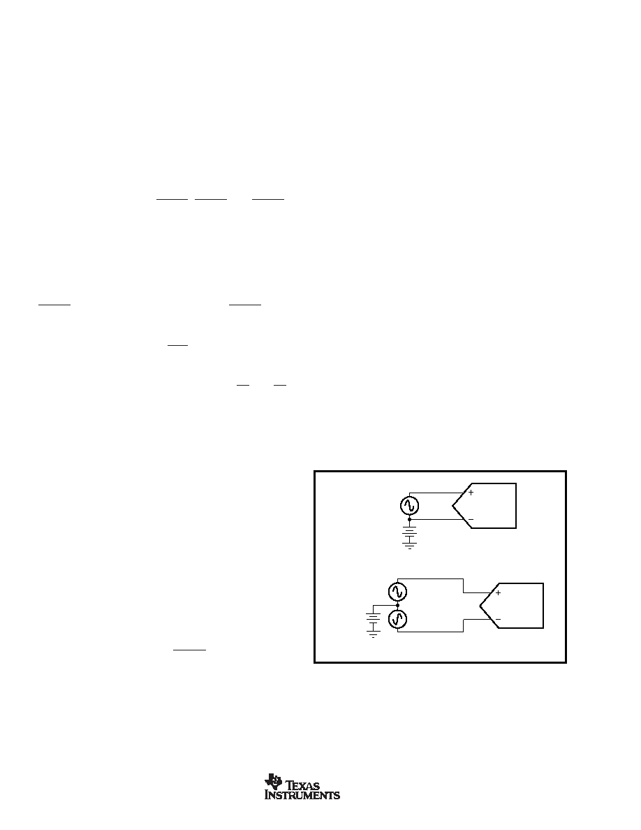
ANALOG INPUT
The analog input is bipolar and fully differential. There are two
general methods of driving the analog input of the ADS8364:
single-ended or differential, as shown in Figure 1 and
Figure 2. When the input is single-ended, the –IN input is held
at the common-mode voltage. The +IN input swings around
the same common voltage and the peak-to-peak amplitude is
the (common-mode + VREF) and the (common-mode – VREF).
The value of VREF determines the range over which the
common-mode voltage may vary (see Figure 3).
FIGURE 1. Methods of Driving the ADS8364 Single-Ended or
Differential.
ADS8364
Single-Ended Input
Common
Voltage
–V
REF to +VREF
peak-to-peak
Differential Input
Common
Voltage
V
REF
peak-to-peak
V
REF
peak-to-peak
相关PDF资料 |
PDF描述 |
|---|---|
| 101A052-3/42-0 | BOOT MOLDED |
| SRR0906-472YL | INDUCTOR PWR 4700UH 15% SHLD SMD |
| EBA14DRMT-S288 | CONN EDGECARD 28POS .125 EXTEND |
| LGU2W221MELA | CAP ALUM 220UF 450V 20% SNAP |
| HFI-160808-R15J | INDUCTOR 1.6X0.8X0.8MM 150NH |
相关代理商/技术参数 |
参数描述 |
|---|---|
| ADS8364M-EVM | 功能描述:数据转换 IC 开发工具 ADC CONVERTER RoHS:否 制造商:Texas Instruments 产品:Demonstration Kits 类型:ADC 工具用于评估:ADS130E08 接口类型:SPI 工作电源电压:- 6 V to + 6 V |
| ADS8364Y | 制造商:TI 制造商全称:Texas Instruments 功能描述:250kHz, 16-Bit, 6-Channel Simultaneous Sampling ANALOG-TO-DIGITAL CONVERTERS |
| ADS8364Y/250 | 功能描述:模数转换器 - ADC 16-Bit 250kSPS 6 ADC Parallel Out RoHS:否 制造商:Texas Instruments 通道数量:2 结构:Sigma-Delta 转换速率:125 SPs to 8 KSPs 分辨率:24 bit 输入类型:Differential 信噪比:107 dB 接口类型:SPI 工作电源电压:1.7 V to 3.6 V, 2.7 V to 5.25 V 最大工作温度:+ 85 C 安装风格:SMD/SMT 封装 / 箱体:VQFN-32 |
| ADS8364Y/250G4 | 功能描述:模数转换器 - ADC 16-Bit 250kSPS 6 ADC Parallel Out RoHS:否 制造商:Texas Instruments 通道数量:2 结构:Sigma-Delta 转换速率:125 SPs to 8 KSPs 分辨率:24 bit 输入类型:Differential 信噪比:107 dB 接口类型:SPI 工作电源电压:1.7 V to 3.6 V, 2.7 V to 5.25 V 最大工作温度:+ 85 C 安装风格:SMD/SMT 封装 / 箱体:VQFN-32 |
| ADS8364Y/2K | 功能描述:模数转换器 - ADC 16-Bit 250kSPS 6 ADC Parallel Out RoHS:否 制造商:Texas Instruments 通道数量:2 结构:Sigma-Delta 转换速率:125 SPs to 8 KSPs 分辨率:24 bit 输入类型:Differential 信噪比:107 dB 接口类型:SPI 工作电源电压:1.7 V to 3.6 V, 2.7 V to 5.25 V 最大工作温度:+ 85 C 安装风格:SMD/SMT 封装 / 箱体:VQFN-32 |
发布紧急采购,3分钟左右您将得到回复。