- 您现在的位置:买卖IC网 > PDF目录17000 > ADS8364EVM (Texas Instruments)EVALUATION MODULE FOR BQ2018 PDF资料下载
参数资料
| 型号: | ADS8364EVM |
| 厂商: | Texas Instruments |
| 文件页数: | 23/26页 |
| 文件大小: | 0K |
| 描述: | EVALUATION MODULE FOR BQ2018 |
| 产品培训模块: | Data Converter Basics |
| 标准包装: | 1 |
| ADC 的数量: | 6 |
| 位数: | 16 |
| 采样率(每秒): | 250k |
| 数据接口: | 并联 |
| 输入范围: | 0 ~ 5 V |
| 在以下条件下的电源(标准): | 413.5mW @ 250kSPS |
| 工作温度: | -40°C ~ 85°C |
| 已用 IC / 零件: | ADS8364 |
| 已供物品: | 板 |
| 相关产品: | 296-13449-6-ND - IC ADC LP 16BIT 250KSPS 64TQFP ADS8364Y/2KG4-ND - IC ADC LP 16BIT 250KSPS 64-TQFP ADS8364Y/2K-ND - IC ADC LP 16BIT 250KSPS 64-TQFP ADS8364Y/250G4-ND - IC ADC LP 16BIT 250KSPS 64-TQFP 296-13449-1-ND - IC ADC LP 16BIT 250KSPS 64TQFP 296-13449-2-ND - IC ADC LP 16BIT 250KSPS 64TQFP |
ADS8364
6
SBAS219C
www.ti.com
SPEC
DESCRIPTION
MIN
TYP(1)
MAX
UNITS
tCONV
Conversion Time
3.2
s
tACQ
Acquistion Time
0.8
s
tC1
Cycle Time of CLK
200
ns
tW1
Pulse Width CLK HIGH Time or LOW Time.
60
ns
tD1(5)
Delay Time of Rising Edge of Clock After Falling Edge of HOLD (A,B,C)
10
ns
tW2
Pulse Width of HOLDX HIGH Time to be Recognized again
BVDD = 5V
15
ns
BVDD = 3V
30
ns
tW3
Pulse Width of HOLDX LOW Time
BVDD = 5V
20
ns
BVDD = 3V
30
ns
tW4
Pulse Width of RESET
BVDD = 5V
20
ns
BVDD = 3V
40
ns
tW5
Pulse Width of RD HIGH Time
BVDD = 5V
30
ns
BVDD = 3V
40
ns
tD2
Delay Time of First Hold After RESET
BVDD = 5V
20
ns
BVDD = 3V
40
ns
tD4
Delay Time of Falling Edge of RD After Falling Edge of CS
0
ns
tD5
Delay Time of Rising Edge of CS After Rising Edge of RD
0
ns
tW6
Pulse Width of RD and CS Both LOW Time
BVDD = 5V
50
ns
BVDD = 3V
70
ns
tW7
Pulse Width of RD HIGH Time
BVDD = 5V
20
ns
BVDD = 3V
40
ns
tD6
Delay Time of Data Valid After Falling Edge RD
BVDD = 5V
40
ns
BVDD = 3V
60
ns
tD7
Delay Time of Data Hold From Rising Edge of RD
BVDD = 5V
5
ns
BVDD = 3V
10
ns
tD8
Delay Time of RD HIGH After CS LOW
BVDD = 5V
50
ns
BVDD = 3V
60
ns
tD9
Delay Time of RD Low After Address Setup
BVDD = 5V
10
ns
BVDD = 3V
20
ns
NOTES: (1) Assured by design. (2) All input signals are specified with tr = tf = 5ns (10% to 90% of BVDD) and timed from a voltage level of (VIL + VIH)/2.
(3) See timing diagram above. (4) BYTE is asynchronous; when BYTE is 0, bits 15 through 0 appear at DB15-DB0. When BYTE is 1, bits 15 through 8
appear on DB7-DB0. RD may remain LOW between changes in BYTE. (5) Only important when synchronization to clock is important.
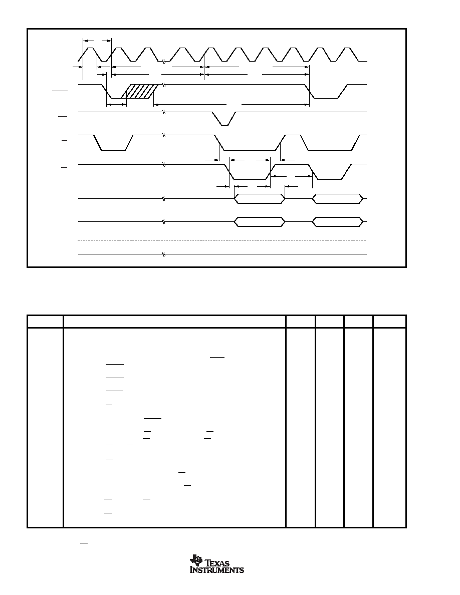
TIMING CHARACTERISTICS TABLE
Timing Characteristics over recommended operating free-air temperature range T
MIN to TMAX, AVDD = DVDD = 5V, REFIN = REFOUT internal reference +2.5V,
f
CLK = 5MHz, fSAMPLE = 250kSPS, BVDD = 2.7 ÷ 5V (unless otherwise noted).
TIMING CHARACTERISTICS
t
W6
t
D6
t
D4
t
D5
t
D7
t
W5
t
W1
t
D1
t
C1
t
W3
CONVERSION
t
CONV
ACQUISITION
t
ACQ
t
W2
Bits 15-8
Bits 7-0
Bits 15-8
Bits 7-0
CLK
HOLDX
EOC
CS
RD
D15-D8
D7-D0
BYTE
1
2
16
17
18
19
20
1
2
相关PDF资料 |
PDF描述 |
|---|---|
| 101A052-3/42-0 | BOOT MOLDED |
| SRR0906-472YL | INDUCTOR PWR 4700UH 15% SHLD SMD |
| EBA14DRMT-S288 | CONN EDGECARD 28POS .125 EXTEND |
| LGU2W221MELA | CAP ALUM 220UF 450V 20% SNAP |
| HFI-160808-R15J | INDUCTOR 1.6X0.8X0.8MM 150NH |
相关代理商/技术参数 |
参数描述 |
|---|---|
| ADS8364M-EVM | 功能描述:数据转换 IC 开发工具 ADC CONVERTER RoHS:否 制造商:Texas Instruments 产品:Demonstration Kits 类型:ADC 工具用于评估:ADS130E08 接口类型:SPI 工作电源电压:- 6 V to + 6 V |
| ADS8364Y | 制造商:TI 制造商全称:Texas Instruments 功能描述:250kHz, 16-Bit, 6-Channel Simultaneous Sampling ANALOG-TO-DIGITAL CONVERTERS |
| ADS8364Y/250 | 功能描述:模数转换器 - ADC 16-Bit 250kSPS 6 ADC Parallel Out RoHS:否 制造商:Texas Instruments 通道数量:2 结构:Sigma-Delta 转换速率:125 SPs to 8 KSPs 分辨率:24 bit 输入类型:Differential 信噪比:107 dB 接口类型:SPI 工作电源电压:1.7 V to 3.6 V, 2.7 V to 5.25 V 最大工作温度:+ 85 C 安装风格:SMD/SMT 封装 / 箱体:VQFN-32 |
| ADS8364Y/250G4 | 功能描述:模数转换器 - ADC 16-Bit 250kSPS 6 ADC Parallel Out RoHS:否 制造商:Texas Instruments 通道数量:2 结构:Sigma-Delta 转换速率:125 SPs to 8 KSPs 分辨率:24 bit 输入类型:Differential 信噪比:107 dB 接口类型:SPI 工作电源电压:1.7 V to 3.6 V, 2.7 V to 5.25 V 最大工作温度:+ 85 C 安装风格:SMD/SMT 封装 / 箱体:VQFN-32 |
| ADS8364Y/2K | 功能描述:模数转换器 - ADC 16-Bit 250kSPS 6 ADC Parallel Out RoHS:否 制造商:Texas Instruments 通道数量:2 结构:Sigma-Delta 转换速率:125 SPs to 8 KSPs 分辨率:24 bit 输入类型:Differential 信噪比:107 dB 接口类型:SPI 工作电源电压:1.7 V to 3.6 V, 2.7 V to 5.25 V 最大工作温度:+ 85 C 安装风格:SMD/SMT 封装 / 箱体:VQFN-32 |
发布紧急采购,3分钟左右您将得到回复。