- 您现在的位置:买卖IC网 > PDF目录2065 > ADS8364Y/250G4 (Texas Instruments)IC ADC LP 16BIT 250KSPS 64-TQFP PDF资料下载
参数资料
| 型号: | ADS8364Y/250G4 |
| 厂商: | Texas Instruments |
| 文件页数: | 6/26页 |
| 文件大小: | 0K |
| 描述: | IC ADC LP 16BIT 250KSPS 64-TQFP |
| 产品培训模块: | Data Converter Basics |
| 标准包装: | 250 |
| 位数: | 16 |
| 采样率(每秒): | 250k |
| 数据接口: | 并联 |
| 转换器数目: | 6 |
| 功率耗散(最大): | 471.5mW |
| 电压电源: | 模拟和数字 |
| 工作温度: | -40°C ~ 85°C |
| 安装类型: | 表面贴装 |
| 封装/外壳: | 64-TQFP |
| 供应商设备封装: | 64-TQFP(10x10) |
| 包装: | 带卷 (TR) |
| 输入数目和类型: | 12 个单端,双极;6 个差分,双极 |
| 配用: | 296-30708-ND - EVAL MODULE FOR ADS8364 ADS8364EVM-ND - EVALUATION MODULE FOR BQ2018 |
ADS8364
14
SBAS219C
www.ti.com
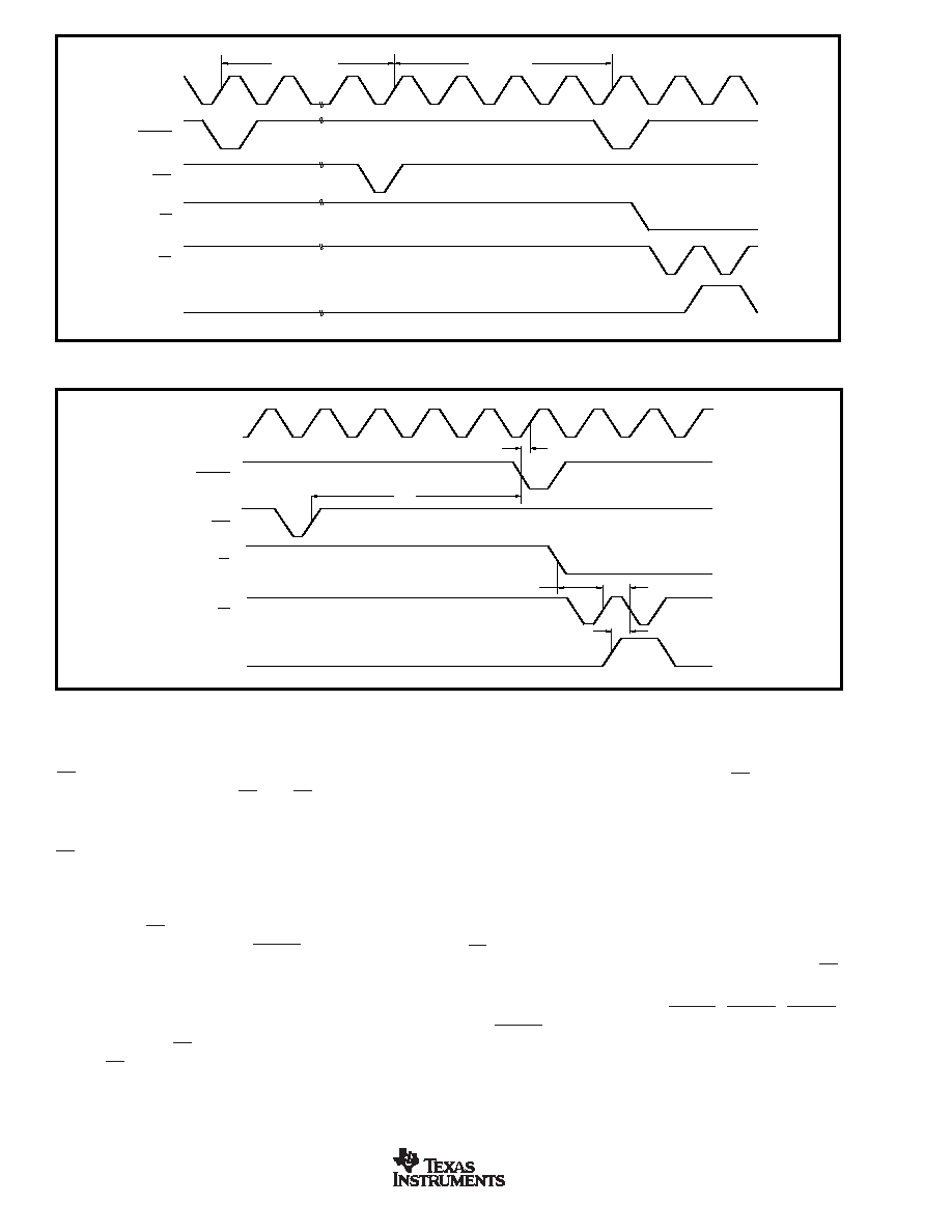
FIGURE 9. Timing for Reading Data.
register, the possibility still exists that the new data was
latched to the output register just before the falling edge of
RD. If a read process is initiated around 16.5 clock cycles
after the conversion started, RD and CS should stay LOW
for at least 50ns (see Timing Diagram, tW6) to get the new
data stored to its register and switched to the output.
CS being LOW tells the ADS8364 that the bus on the board
is assigned to the ADS8364. If an ADC shares a bus with
digital gates, there is a possibility that digital (high-frequency)
noise will be coupled into the ADC. If the bus is just used by
the ADS8364, CS can be hardwired to ground. Reading data
at the falling edge of one of the HOLDX signals might cause
noise.
BYTE—If there is only an 8-bit bus available on a board,
then BYTE can be set HIGH. (see Figure 11) In this case, the
lower 8 bits can be read at the output pins D15 to D8 or D7
to D0 at the first RD signal and the higher bits after the
second RD signal. If the ADS8364 is used in the cycle or the
FIFO mode, then the address and a data valid information is
added to the data if ADD is HIGH. In this case, the address will
be read first, then the lower 8 bits, and finally the higher 8 bits.
FIGURE 8. Timing of one Conversion Cycle.
If BYTE is LOW, then the ADS8364 operates in the 16-bit
output mode. Here, data is read between the pins DB15 and
DB0. As long as ADD is LOW, with every RD-impulse, data
from a new channel is brought to the output. If ADD is HIGH,
and the cycle or the FIFO mode is chosen; the first output
word will contain the address, while the second output word
contains the 16-bit data.
ADD-Signal–In the cycle and the FIFO mode, it might be
desirable to have address information with the 16-bit output
data. Therefore, ADD can be set HIGH. In this case, two (or
three readings if the part is operated with byte being HIGH)
RD-signals are necessary to read data of one channel, while
the ADS8364 provides channel information on the first RD
signal (see Table III and Table IV).
The signals ADD, A0, A1, A2, RESET, HOLDA, HOLDB,
and HOLDC are accessible through the data bus and control
word. All these pins are in OR configuration with hardware
pins. When software configuration is used, the correspond-
ing pins must be connected to ground or the power supply.
When the MSB is HIGH, the device is in the configuration
mode. MSB LOW will start conversion or reset the part.
1
2
16
17
18
19
20
1
2
CONVERSION
ACQUISITION
CLK
HOLD B
EOC
CS
RD
A0
t
ACQ
t
D1
t
D8
t
W7
16
17
18
19
20
1
2
CLK
HOLD X
EOC
CS
RD
A0
t
D9
相关PDF资料 |
PDF描述 |
|---|---|
| ADS8412IPFBRG4 | IC ADC 16BIT 2MSPS 48-TQFP |
| ADV7180WBCPZ | IC VIDEO DECODER SDTV 40LFCSP |
| ADV7186BBCZ | IC VIDEO DECODER 196CSPBGA |
| ADV7441ABSTZ-5P | IC DECODER DIGITIZER 144LQFP |
| ADV7513BSWZ | IC TX HDMI 165MHZ 64LQFP |
相关代理商/技术参数 |
参数描述 |
|---|---|
| ADS8365 | 制造商:BB 制造商全称:BB 功能描述:16-Bit, 250kSPS, 6-Channel, Simultaneous Sampling SAR ANALOG-TO-DIGITAL CONVERTERS |
| ADS8365IPAG | 功能描述:模数转换器 - ADC 16B 250kSPS 6Ch Simu Sampling SAR ADC RoHS:否 制造商:Texas Instruments 通道数量:2 结构:Sigma-Delta 转换速率:125 SPs to 8 KSPs 分辨率:24 bit 输入类型:Differential 信噪比:107 dB 接口类型:SPI 工作电源电压:1.7 V to 3.6 V, 2.7 V to 5.25 V 最大工作温度:+ 85 C 安装风格:SMD/SMT 封装 / 箱体:VQFN-32 |
| ADS8365IPAGG4 | 功能描述:模数转换器 - ADC 16B 250kSPS 6Ch Simu Sampling SAR ADC RoHS:否 制造商:Texas Instruments 通道数量:2 结构:Sigma-Delta 转换速率:125 SPs to 8 KSPs 分辨率:24 bit 输入类型:Differential 信噪比:107 dB 接口类型:SPI 工作电源电压:1.7 V to 3.6 V, 2.7 V to 5.25 V 最大工作温度:+ 85 C 安装风格:SMD/SMT 封装 / 箱体:VQFN-32 |
| ADS8365IPAGG-4 | 制造商:Texas Instruments 功能描述:IC, SM 16-BIT ADC 6CH SAR |
| ADS8365IPAGR | 功能描述:模数转换器 - ADC 16 B 250k SPS 6 Ch Smltns Smplg SARADC RoHS:否 制造商:Texas Instruments 通道数量:2 结构:Sigma-Delta 转换速率:125 SPs to 8 KSPs 分辨率:24 bit 输入类型:Differential 信噪比:107 dB 接口类型:SPI 工作电源电压:1.7 V to 3.6 V, 2.7 V to 5.25 V 最大工作温度:+ 85 C 安装风格:SMD/SMT 封装 / 箱体:VQFN-32 |
发布紧急采购,3分钟左右您将得到回复。