- 您现在的位置:买卖IC网 > PDF目录19369 > ADSP-21060KSZ-133 (Analog Devices Inc)IC DSP CONTROLLER 32BIT 240-MQFP PDF资料下载
参数资料
| 型号: | ADSP-21060KSZ-133 |
| 厂商: | Analog Devices Inc |
| 文件页数: | 20/64页 |
| 文件大小: | 0K |
| 描述: | IC DSP CONTROLLER 32BIT 240-MQFP |
| 产品培训模块: | SHARC Processor Overview |
| 标准包装: | 1 |
| 系列: | SHARC® |
| 类型: | 浮点 |
| 接口: | 主机接口,连接端口,串行端口 |
| 时钟速率: | 33MHz |
| 非易失内存: | 外部 |
| 芯片上RAM: | 512kB |
| 电压 - 输入/输出: | 5.00V |
| 电压 - 核心: | 5.00V |
| 工作温度: | 0°C ~ 85°C |
| 安装类型: | 表面贴装 |
| 封装/外壳: | 240-BFQFP 裸露焊盘 |
| 供应商设备封装: | 240-MQFP-EP(32x32) |
| 包装: | 托盘 |
第1页第2页第3页第4页第5页第6页第7页第8页第9页第10页第11页第12页第13页第14页第15页第16页第17页第18页第19页当前第20页第21页第22页第23页第24页第25页第26页第27页第28页第29页第30页第31页第32页第33页第34页第35页第36页第37页第38页第39页第40页第41页第42页第43页第44页第45页第46页第47页第48页第49页第50页第51页第52页第53页第54页第55页第56页第57页第58页第59页第60页第61页第62页第63页第64页
ADSP-21060/ADSP-21060L/ADSP-21062/ADSP-21062L/ADSP-21060C/ADSP-21060LC
Rev. F
|
Page 27 of 64
|
March 2008
Synchronous Read/Write—Bus Master
Use these specifications for interfacing to external memory sys-
tems that require CLKIN—relative timing or for accessing a
slave ADSP-2106x (in multiprocessor memory space). These
synchronous switching characteristics are also valid during
asynchronous memory reads and writes except where noted (see
Bus Master on Page 26). When accessing a slave ADSP-2106x,
these switching characteristics must meet the slave’s timing
requirements for synchronous read/writes (see Synchronous
Read/Write—Bus Slave on Page 29). The slave ADSP-2106x
must also meet these (bus master) timing requirements for data
and acknowledge setup and hold times.
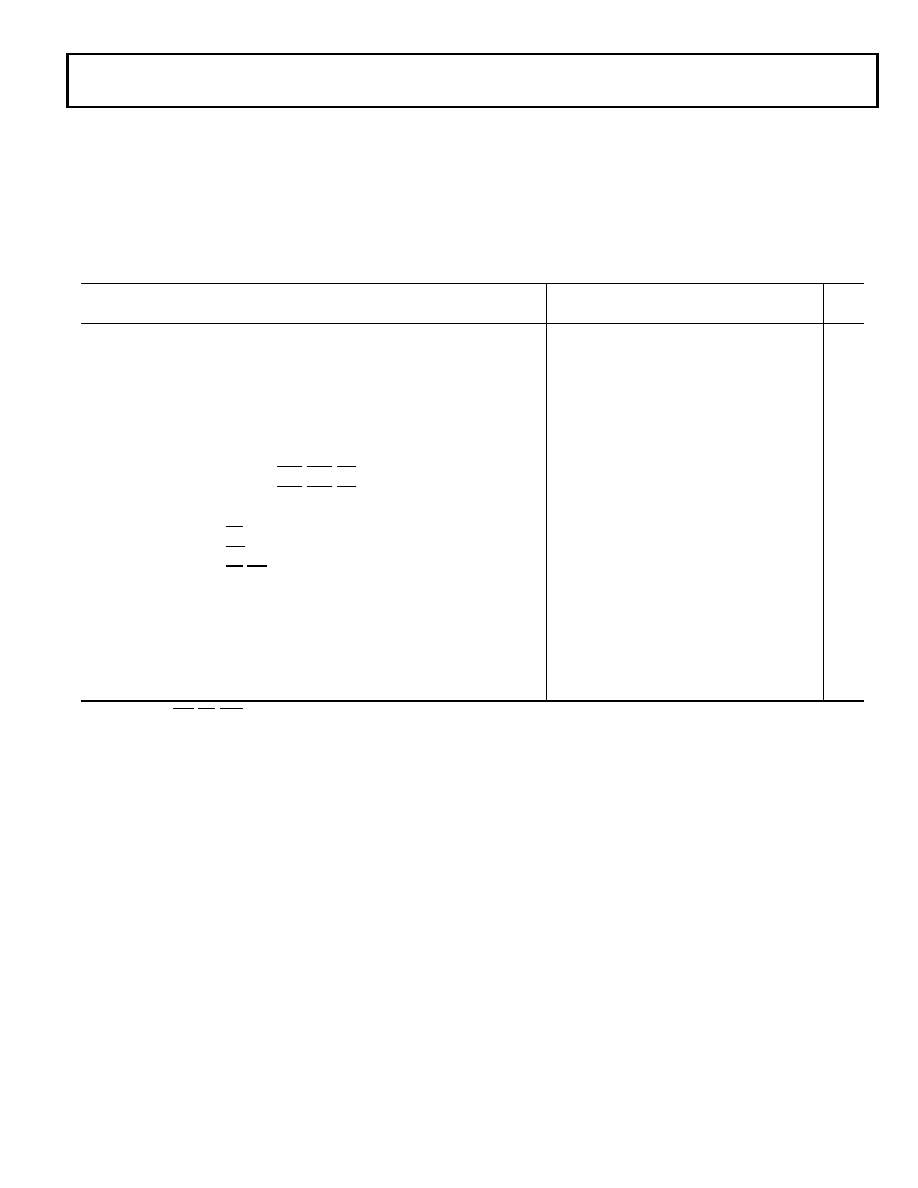
Table 16. Synchronous Read/Write—Bus Master
5 V and 3.3 V
Unit
Parameter
Min
Max
Timing Requirements
tSSDATI
Data Setup Before CLKIN
3 + DT/8
ns
tHSDATI
Data Hold After CLKIN
3.5 – DT/8
ns
tDAAK
ACK Delay After Address, Selects1, 2
14 + 7DT/8 + W
ns
tSACKC
ACK Setup Before CLKIN2
6.5 + DT/4
ns
tHACK
ACK Hold After CLKIN
–1 – DT/4
ns
Switching Characteristics
tDADRO
Address, MSx, BMS, SW Delay After CLKIN1
7 – DT/8
ns
tHADRO
Address, MSx, BMS, SW Hold After CLKIN
–1 – DT/8
ns
tDPGC
PAGE Delay After CLKIN
9 + DT/8
16 + DT/8
ns
tDRDO
RD High Delay After CLKIN
–2 – DT/8
4 – DT/8
ns
tDWRO
WR High Delay After CLKIN
–3 – 3DT/16
4 – 3DT/16
ns
tDRWL
RD/WR Low Delay After CLKIN
8 + DT/4
12.5 + DT/4
ns
tSDDATO
Data Delay After CLKIN
19 + 5DT/16
ns
tDATTR
Data Disable After CLKIN3
0 – DT/8
7 – DT/8
ns
tDADCCK
ADRCLK Delay After CLKIN
4 + DT/8
10 + DT/8
ns
tADRCK
ADRCLK Period
tCK
ns
tADRCKH
ADRCLK Width High
(tCK/2 – 2)
ns
tADRCKL
ADRCLK Width Low
(tCK/2 – 2)
ns
1 The falling edge of MSx, SW, BMS is referenced.
2 ACK delay/setup: user must meet tDAAK or tDSAK or synchronous specification tSAKC for deassertion of ACK (low), all three specifications must be met for assertion of ACK
(high).
3 See Example System Hold Time Calculation on Page 47 for calculation of hold times given capacitive and dc loads.
相关PDF资料 |
PDF描述 |
|---|---|
| EBC25DRTS | CONN EDGECARD 50POS DIP .100 SLD |
| VE-B3D-CY-S | CONVERTER MOD DC/DC 85V 50W |
| TPSD686K020R0200 | CAP TANT 68UF 20V 10% 2917 |
| VI-B3Y-CX-F4 | CONVERTER MOD DC/DC 3.3V 49.5W |
| VE-B3B-CY-S | CONVERTER MOD DC/DC 95V 50W |
相关代理商/技术参数 |
参数描述 |
|---|---|
| ADSP-21060KSZ-160 | 功能描述:IC DSP CONTROLLER 32BIT 240MQFP RoHS:是 类别:集成电路 (IC) >> 嵌入式 - DSP(数字式信号处理器) 系列:SHARC® 标准包装:40 系列:TMS320DM64x, DaVinci™ 类型:定点 接口:I²C,McASP,McBSP 时钟速率:400MHz 非易失内存:外部 芯片上RAM:160kB 电压 - 输入/输出:3.30V 电压 - 核心:1.20V 工作温度:0°C ~ 90°C 安装类型:表面贴装 封装/外壳:548-BBGA,FCBGA 供应商设备封装:548-FCBGA(27x27) 包装:托盘 配用:TMDSDMK642-0E-ND - DEVELPER KIT W/NTSC CAMERA296-23038-ND - DSP STARTER KIT FOR TMS320C6416296-23059-ND - FLASHBURN PORTING KIT296-23058-ND - EVAL MODULE FOR DM642TMDSDMK642-ND - DEVELOPER KIT W/NTSC CAMERA |
| ADSP21060L | 制造商:AD 制造商全称:Analog Devices 功能描述:DSP MICROCOMPUTER |
| ADSP-21060L | 制造商:AD 制造商全称:Analog Devices 功能描述:ADSP-2106x SHARC DSP Microcomputer Family |
| ADSP-21060LAB-160 | 功能描述:IC DSP CONTROLLER 32BIT 225BGA RoHS:否 类别:集成电路 (IC) >> 嵌入式 - DSP(数字式信号处理器) 系列:SHARC® 标准包装:2 系列:StarCore 类型:SC140 内核 接口:DSI,以太网,RS-232 时钟速率:400MHz 非易失内存:外部 芯片上RAM:1.436MB 电压 - 输入/输出:3.30V 电压 - 核心:1.20V 工作温度:-40°C ~ 105°C 安装类型:表面贴装 封装/外壳:431-BFBGA,FCBGA 供应商设备封装:431-FCPBGA(20x20) 包装:托盘 |
| ADSP-21060LABZ-160 | 功能描述:IC DSP CONTROLLER 32BIT 225-BGA RoHS:是 类别:集成电路 (IC) >> 嵌入式 - DSP(数字式信号处理器) 系列:SHARC® 标准包装:2 系列:StarCore 类型:SC140 内核 接口:DSI,以太网,RS-232 时钟速率:400MHz 非易失内存:外部 芯片上RAM:1.436MB 电压 - 输入/输出:3.30V 电压 - 核心:1.20V 工作温度:-40°C ~ 105°C 安装类型:表面贴装 封装/外壳:431-BFBGA,FCBGA 供应商设备封装:431-FCPBGA(20x20) 包装:托盘 |
发布紧急采购,3分钟左右您将得到回复。