- 您现在的位置:买卖IC网 > PDF目录19400 > ADSP-21479KBCZ-1A (Analog Devices Inc)IC DSP SHARK 200MHZ 196CSPBGA PDF资料下载
参数资料
| 型号: | ADSP-21479KBCZ-1A |
| 厂商: | Analog Devices Inc |
| 文件页数: | 20/76页 |
| 文件大小: | 0K |
| 描述: | IC DSP SHARK 200MHZ 196CSPBGA |
| 标准包装: | 1 |
| 系列: | SHARC® |
| 类型: | 浮点 |
| 接口: | DAI,DPI,EBI/EMI,I²C,SPI,SPORT,UART/USART |
| 时钟速率: | 200MHz |
| 非易失内存: | ROM(4Mb) |
| 芯片上RAM: | 5Mb |
| 电压 - 输入/输出: | 3.30V |
| 电压 - 核心: | 1.20V |
| 工作温度: | 0°C ~ 70°C |
| 安装类型: | 表面贴装 |
| 封装/外壳: | 196-LFBGA,CSPBGA |
| 供应商设备封装: | 196-CSPBGA(12x12) |
| 包装: | 托盘 |
第1页第2页第3页第4页第5页第6页第7页第8页第9页第10页第11页第12页第13页第14页第15页第16页第17页第18页第19页当前第20页第21页第22页第23页第24页第25页第26页第27页第28页第29页第30页第31页第32页第33页第34页第35页第36页第37页第38页第39页第40页第41页第42页第43页第44页第45页第46页第47页第48页第49页第50页第51页第52页第53页第54页第55页第56页第57页第58页第59页第60页第61页第62页第63页第64页第65页第66页第67页第68页第69页第70页第71页第72页第73页第74页第75页第76页
Rev. C
|
Page 27 of 76
|
July 2013
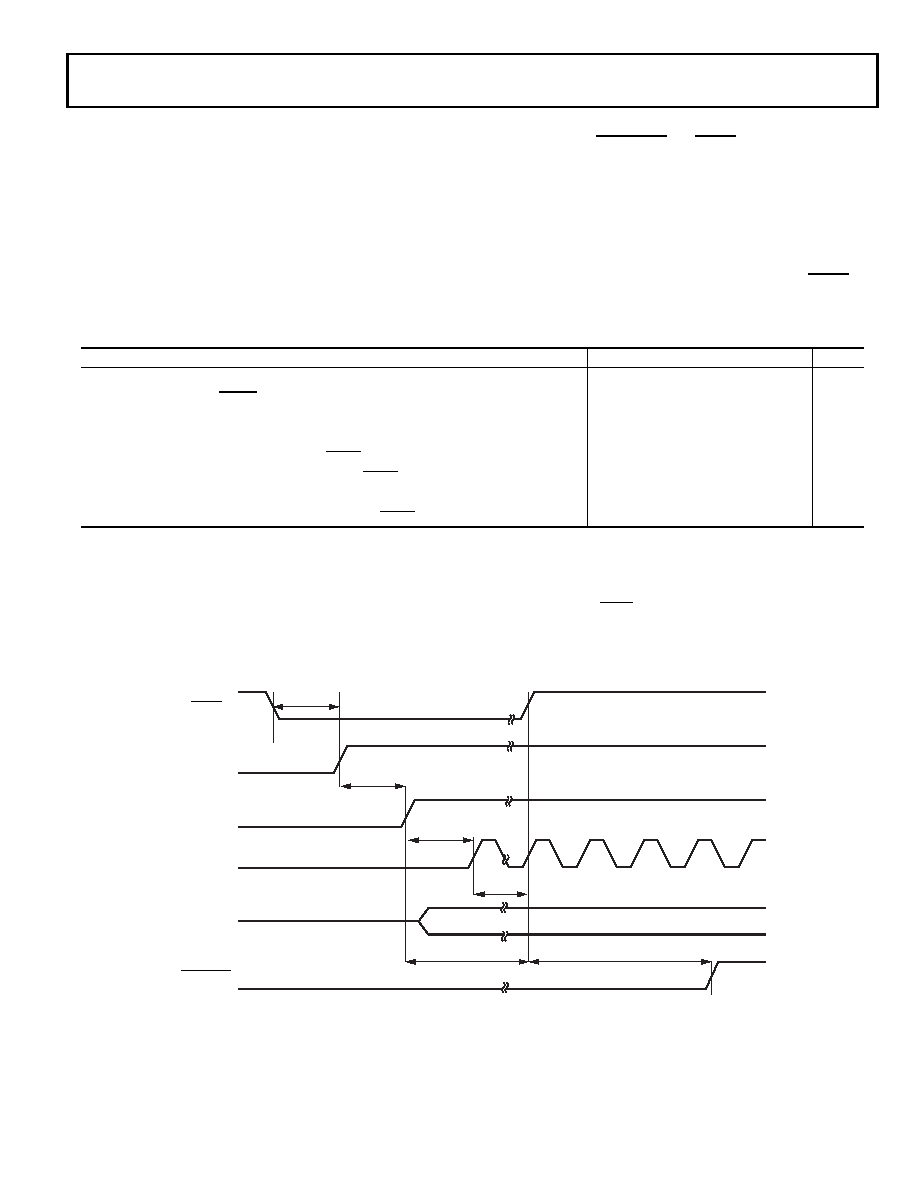
Power-Up Sequencing
The timing requirements for processor startup are given in
Table 19. While no specific power-up sequencing is required
between VDD_EXT and VDD_INT, there are some considerations
that the system designs should take into account.
No power supply should be powered up for an extended
period of time (>200 ms) before another supply starts to
ramp up.
If the VDD_INT power supply comes up after VDD_EXT, any
pin, such as RESETOUT and RESET, may actually drive
momentarily until the VDD_INT rail has powered up. Systems
sharing these signals on the board must determine if there
are any issues that need to be addressed based on this
behavior.
Note that during power-up, when the VDD_INT power supply
comes up after VDD_EXT, a leakage current of the order of three-
state leakage current pull-up, pull-down, may be observed on
any pin, even if that is an input only (for example, the RESET
pin), until the VDD_INT rail has powered up.
Table 19. Power-Up Sequencing Timing Requirements (Processor Startup)
Parameter
Min
Max
Unit
Timing Requirements
tRSTVDD
RESET Low Before VDD_EXT or VDD_INT On
0
ms
tIVDDEVDD
VDD_INT On Before VDD_EXT
–200
+200
ms
tCLKVDD
1
CLKIN Valid After VDD_INT and VDD_EXT Valid
0
200
ms
tCLKRST
CLKIN Valid Before RESET Deasserted
10
2
μs
tPLLRST
PLL Control Setup Before RESET Deasserted
203
μs
Switching Characteristic
tCORERST
Core Reset Deasserted After RESET Deasserted
4096 × tCK + 2 × tCCLK
4, 5
1 Valid V
DD_INT and VDD_EXT assumes that the supplies are fully ramped to their nominal values (it does not matter which supply comes up first). Voltage ramp rates can vary
from microseconds to hundreds of milliseconds depending on the design of the power supply subsystem.
2 Assumes a stable CLKIN signal, after meeting worst-case startup timing of crystal oscillators. Refer to your crystal oscillator manufacturer's data sheet for startup time. Assume
a 25 ms maximum oscillator startup time if using the XTAL pin and internal oscillator circuit in conjunction with an external crystal.
3 Based on CLKIN cycles.
4 Applies after the power-up sequence is complete. Subsequent resets require a minimum of four CLKIN cycles for RESET to be held low in order to properly initialize and
propagate default states at all I/O pins.
5 The 4096 cycle count depends on tSRST specification in Table 21. If setup time is not met, one additional CLKIN cycle may be added to the core reset time, resulting in 4097
cycles maximum.
Figure 6. Power-Up Sequencing
tRSTVDD
tCLKVDD
tCLKRST
tCORERST
tPLLRST
VDDEXT
VDDINT
CLKIN
CLK_CFG1–0
RESET
RESETOUT
tIVDDEVDD
相关PDF资料 |
PDF描述 |
|---|---|
| MLP2520S2R2S | INDUCTOR MULTILAYER 2.2UH 1008 |
| MAX6518UKP035+T | IC TEMP SENSOR SW SOT23-5 |
| VI-23D-CY-F1 | CONVERTER MOD DC/DC 85V 50W |
| GEC12DRXH-S734 | CONN EDGECARD 24POS DIP .100 SLD |
| VI-B6J-EU-B1 | CONVERTER MOD DC/DC 36V 200W |
相关代理商/技术参数 |
参数描述 |
|---|---|
| ADSP-21479KBCZ-2A | 功能描述:IC DSP SHARC 266MHZ LP 196CSPBGA RoHS:是 类别:集成电路 (IC) >> 嵌入式 - DSP(数字式信号处理器) 系列:SHARC® 标准包装:2 系列:StarCore 类型:SC140 内核 接口:DSI,以太网,RS-232 时钟速率:400MHz 非易失内存:外部 芯片上RAM:1.436MB 电压 - 输入/输出:3.30V 电压 - 核心:1.20V 工作温度:-40°C ~ 105°C 安装类型:表面贴装 封装/外壳:431-BFBGA,FCBGA 供应商设备封装:431-FCPBGA(20x20) 包装:托盘 |
| ADSP-21479KBCZ-3A | 功能描述:IC DSP SHARK 300MHZ 196CSPBGA RoHS:是 类别:集成电路 (IC) >> 嵌入式 - DSP(数字式信号处理器) 系列:SHARC® 标准包装:2 系列:StarCore 类型:SC140 内核 接口:DSI,以太网,RS-232 时钟速率:400MHz 非易失内存:外部 芯片上RAM:1.436MB 电压 - 输入/输出:3.30V 电压 - 核心:1.20V 工作温度:-40°C ~ 105°C 安装类型:表面贴装 封装/外壳:431-BFBGA,FCBGA 供应商设备封装:431-FCPBGA(20x20) 包装:托盘 |
| ADSP-21479KBCZ-3AX | 制造商:Analog Devices 功能描述:- Trays |
| ADSP-21479KBCZ-ENG | 制造商:Analog Devices 功能描述:SHARC PROCESSOR - Trays |
| ADSP-21479KCPZ-1A | 功能描述:IC DSP SHARK 200MHZ 88LFCSP RoHS:是 类别:集成电路 (IC) >> 嵌入式 - DSP(数字式信号处理器) 系列:SHARC® 标准包装:2 系列:StarCore 类型:SC140 内核 接口:DSI,以太网,RS-232 时钟速率:400MHz 非易失内存:外部 芯片上RAM:1.436MB 电压 - 输入/输出:3.30V 电压 - 核心:1.20V 工作温度:-40°C ~ 105°C 安装类型:表面贴装 封装/外壳:431-BFBGA,FCBGA 供应商设备封装:431-FCPBGA(20x20) 包装:托盘 |
发布紧急采购,3分钟左右您将得到回复。