- 您现在的位置:买卖IC网 > PDF目录19380 > ADSP-2183KCAZ-210 (Analog Devices Inc)IC DSP 16BIT 52MHZ 144-BGA PDF资料下载
参数资料
| 型号: | ADSP-2183KCAZ-210 |
| 厂商: | Analog Devices Inc |
| 文件页数: | 28/31页 |
| 文件大小: | 0K |
| 描述: | IC DSP 16BIT 52MHZ 144-BGA |
| 标准包装: | 1 |
| 系列: | ADSP-21xx |
| 类型: | 定点 |
| 接口: | 同步串行端口(SSP) |
| 时钟速率: | 52MHz |
| 非易失内存: | 外部 |
| 芯片上RAM: | 80kB |
| 电压 - 输入/输出: | 3.30V |
| 电压 - 核心: | 3.30V |
| 工作温度: | 0°C ~ 70°C |
| 安装类型: | 表面贴装 |
| 封装/外壳: | 144-LFBGA |
| 供应商设备封装: | 144-迷你型BGA |
| 包装: | 托盘 |
第1页第2页第3页第4页第5页第6页第7页第8页第9页第10页第11页第12页第13页第14页第15页第16页第17页第18页第19页第20页第21页第22页第23页第24页第25页第26页第27页当前第28页第29页第30页第31页
ADSP-2183
–6–
REV. C
When the IDLE (n) instruction is used, it effectively slows down
the processor’s internal clock, and thus its response time, to
incoming interrupts. The one-cycle response time of the stan-
dard idle state is increased by n, the clock divisor. When an
enabled interrupt is received, the ADSP-2183 will remain in the
idle state for up to a maximum of n processor cycles (n = 16, 32,
64 or 128) before resuming normal operation.
When the IDLE (n) instruction is used in systems with an exter-
nally generated serial clock (SCLK), the serial clock rate may be
faster than the processor’s reduced internal clock rate. Under
these conditions, interrupts must not be generated at a faster
rate than can be serviced, due to the additional time the processor
takes to come out of the idle state (a maximum of n processor
cycles).
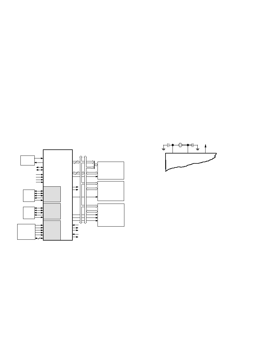
SYSTEM INTERFACE
Figure 2 shows a typical basic system configuration with the
ADSP-2183, two serial devices, a byte-wide EPROM and
optional external program and data overlay memories. Program-
mable wait state generation allows the processor to connect
easily to slow peripheral devices. The ADSP-2183 also provides
four external interrupts and two serial ports or six external inter-
rupts and one serial port.
1/2x CLOCK
OR
CRYSTAL
SERIAL
DEVICE
SERIAL
DEVICE
16
A0-A21
DATA
CS
BYTE
MEMORY
I/O
SPACE
(PERIPHERALS)
CS
DATA
ADDR
DATA
ADDR
2048 LOCATIONS
OVERLAY
MEMORY
TWO 8K
PM SEGMENTS
TWO 8K
DM SEGMENTS
D23-0
A13-0
D23-8
A10-0
D15-8
D23-16
A13-0
14
24
SPORT1
SCLK0
RFS0
TFS0
DT0
DR0
SPORT0
IRD
IWR
IS
IAL
IACK
IAD15-0
IDMA PORT
FL0-2
PF0-7
CLKIN
XTAL
ADDR13-0
DATA23-0
BMS
IOMS
PMS
DMS
CMS
BR
BG
BGH
PWD
PWDACK
ADSP-2183
RD
WR
IRQ2
IRQE
IRQL0
IRQL1
SCLK1
RFS1 OR
IRQ0
TFS1 OR
IRQ1
DT1 OR FO
DR1 OR FI
SYSTEM
INTERFACE
OR
CONTROLLER
Figure 2. ADSP-2183 Basic System Configuration
Clock Signals
The ADSP-2183 can be clocked by either a crystal or a TTL-
compatible clock signal.
The CLKIN input cannot be halted, changed during operation
or operated below the specified frequency during normal opera-
tion. The only exception is while the processor is in the power-
down state. For additional information, refer to Chapter 9,
ADSP-2100 Family User’s Manual, Third Edition, for detailed
information on this power-down feature.
If an external clock is used, it should be a TTL-compatible
signal running at half the instruction rate. The signal is con-
nected to the processor’s CLKIN input. When an external clock
is used, the XTAL input must be left unconnected.
The ADSP-2183 uses an input clock with a frequency equal to
half the instruction rate; a 16.67 MHz input clock yields a 30 ns
processor cycle (which is equivalent to 33 MHz). Normally,
instructions are executed in a single processor cycle. All device
timing is relative to the internal instruction clock rate, which is
indicated by the CLKOUT signal when enabled.
Because the ADSP-2183 includes an on-chip oscillator circuit,
an external crystal may be used. The crystal should be connected
across the CLKIN and XTAL pins, with two capacitors connected
as shown in Figure 3. Capacitor values are dependent on crystal
type and should be specified by the crystal manufacturer. A
parallel-resonant, fundamental frequency, microprocessor-grade
crystal should be used.
A clock output (CLKOUT) signal is generated by the processor
at the processor’s cycle rate. This can be enabled and disabled
by the CLKODIS bit in the SPORT0 Autobuffer Control
Register.
CLKIN
CLKOUT
XTAL
DSP
Figure 3. External Crystal Connections
Reset
The
RESET signal initiates a master reset of the ADSP-2183.
The
RESET signal must be asserted during the power-up se-
quence to assure proper initialization.
RESET during initial
power-up must be held long enough to allow the internal clock
to stabilize. If
RESET is activated any time after power-up, the
clock continues to run and does not require stabilization time.
The power-up sequence is defined as the total time required for
the crystal oscillator circuit to stabilize after a valid VDD is ap-
plied to the processor, and for the internal phase-locked loop
(PLL) to lock onto the specific crystal frequency. A minimum of
2000 CLKIN cycles ensures that the PLL has locked, but does
not include the crystal oscillator start-up time. During this
power-up sequence the
RESET signal should be held low. On
any subsequent resets, the
RESET signal must meet the mini-
mum pulsewidth specification, tRSP.
The
RESET input contains some hysteresis; however, if you use
an RC circuit to generate your
RESET signal, the use of an
external Schmidt trigger is recommended.
The master reset sets all internal stack pointers to the empty
stack condition, masks all interrupts and clears the MSTAT
register. When
RESET is released, if there is no pending bus
request and the chip is configured for booting (MMAP = 0), the
boot-loading sequence is performed. The first instruction is
fetched from on-chip program memory location 0x0000 once
boot loading completes.
相关PDF资料 |
PDF描述 |
|---|---|
| MAX6670AUB50+T | IC TEMP SENSOR REMOTE 10-UMAX |
| MC7824CT | IC REG LDO 24V 1A TO220AB |
| GBC07DRTS | CONN EDGECARD 14POS DIP .100 SLD |
| ABE35DHRR | CONN CARD EXTEND 70POS 1MM SLD |
| RSC35DRSD-S273 | CONN EDGECARD 70POS DIP .100 SLD |
相关代理商/技术参数 |
参数描述 |
|---|---|
| ADSP2183KS133 | 制造商:AD 功能描述:* |
| ADSP-2183KST-115 | 制造商:AD 制造商全称:Analog Devices 功能描述:DSP Microcomputer |
| ADSP-2183KST-133 | 制造商:Analog Devices 功能描述:DSP Fixed-Point 16-Bit 33.3MHz 33.3MIPS 128-Pin LQFP 制造商:Rochester Electronics LLC 功能描述:3.3V 16BITDSP,33MIPS,16KWRDSPM/DM,128TQF - Bulk |
| ADSP-2183KST-160 | 制造商:Analog Devices 功能描述:DSP Fixed-Point 16-Bit 40MHz 40MIPS 128-Pin LQFP 制造商:Rochester Electronics LLC 功能描述:3.3V,16BITDSP,40MIPS,16KWRDSPM/DM,128TQF - Bulk |
| ADSP-2183KST-210 | 制造商:Analog Devices 功能描述:DSP Fixed-Point 16-Bit 52MHz 52MIPS 128-Pin LQFP 制造商:Rochester Electronics LLC 功能描述:3.3V 16BITDSP,52MIPS,16KWORDSPM/DM,128TQ - Bulk 制造商:Analog Devices 功能描述:Digital Signal Processor IC |
发布紧急采购,3分钟左右您将得到回复。