- 您现在的位置:买卖IC网 > PDF目录19395 > ADSP-2185MKSTZ-300 (Analog Devices Inc)IC DSP CONTROLLER 16BIT 100-LQFP PDF资料下载
参数资料
| 型号: | ADSP-2185MKSTZ-300 |
| 厂商: | Analog Devices Inc |
| 文件页数: | 34/40页 |
| 文件大小: | 0K |
| 描述: | IC DSP CONTROLLER 16BIT 100-LQFP |
| 标准包装: | 1 |
| 系列: | ADSP-21xx |
| 类型: | 定点 |
| 接口: | 主机接口,串行端口 |
| 时钟速率: | 75MHz |
| 非易失内存: | 外部 |
| 芯片上RAM: | 80kB |
| 电压 - 输入/输出: | 3.30V |
| 电压 - 核心: | 2.50V |
| 工作温度: | 0°C ~ 70°C |
| 安装类型: | 表面贴装 |
| 封装/外壳: | 100-LQFP |
| 供应商设备封装: | 100-LQFP(14x14) |
| 包装: | 托盘 |
| 其它名称: | ADSP-2185MKSTZ300 |
第1页第2页第3页第4页第5页第6页第7页第8页第9页第10页第11页第12页第13页第14页第15页第16页第17页第18页第19页第20页第21页第22页第23页第24页第25页第26页第27页第28页第29页第30页第31页第32页第33页当前第34页第35页第36页第37页第38页第39页第40页
REV. 0
–4–
ADSP-2185M
ARCHITECTURE OVERVIEW
The ADSP-2185M instruction set provides flexible data moves
and multifunction (one or two data moves with a computation)
instructions. Every instruction can be executed in a single
processor cycle. The ADSP-2185M assembly language uses an
algebraic syntax for ease of coding and readability. A compre-
hensive set of development tools supports program development.
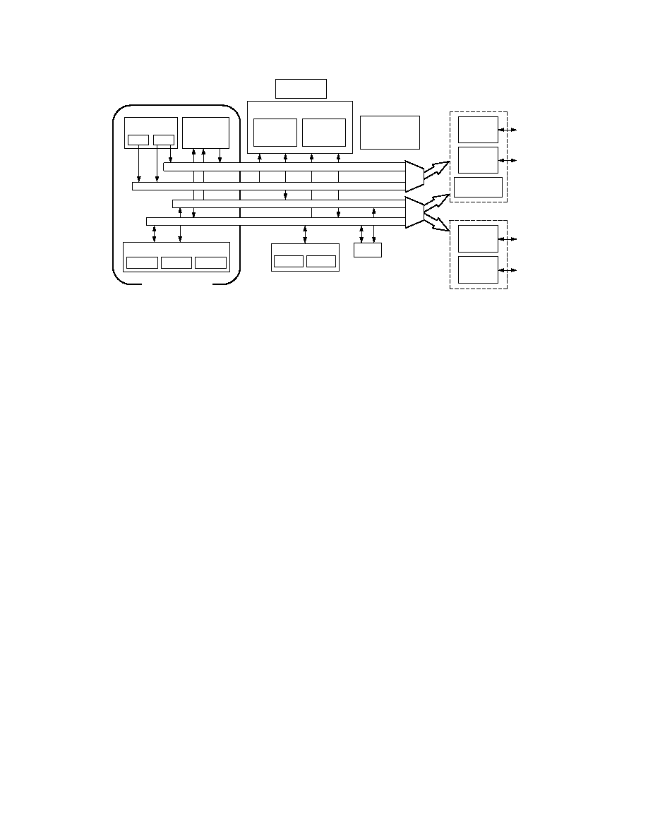
Figure 1 is an overall block diagram of the ADSP-2185M. The
processor contains three independent computational units:
the ALU, the multiplier/accumulator (MAC), and the shifter.
The computational units process 16-bit data directly and have
provisions to support multiprecision computations. The ALU
performs a standard set of arithmetic and logic operations;
division primitives are also supported. The MAC performs
single-cycle multiply, multiply/add, and multiply/subtract opera-
tions with 40 bits of accumulation. The shifter performs logical
and arithmetic shifts, normalization, denormalization, and
derive exponent operations.
The shifter can be used to efficiently implement numeric
format control, including multiword and block floating-point
representations.
The internal result (R) bus connects the computational units so
that the output of any unit may be the input of any unit on the
next cycle.
A powerful program sequencer and two dedicated data address
generators ensure efficient delivery of operands to these computa-
tional units. The sequencer supports conditional jumps, subroutine
calls, and returns in a single cycle. With internal loop counters
and loop stacks, the ADSP-2185M executes looped code with
zero overhead; no explicit jump instructions are required to
maintain loops.
Two data address generators (DAGs) provide addresses for
simultaneous dual operand fetches (from data memory and
program memory). Each DAG maintains and updates four
address pointers. Whenever the pointer is used to access data
(indirect addressing), it is post-modified by the value of one of
four possible modify registers. A length value may be associated
with each pointer to implement automatic modulo addressing
for circular buffers.
Efficient data transfer is achieved with the use of five
internal buses:
Program Memory Address (PMA) Bus
Program Memory Data (PMD) Bus
Data Memory Address (DMA) Bus
Data Memory Data (DMD) Bus
Result (R) Bus
The two address buses (PMA and DMA) share a single external
address bus, allowing memory to be expanded off-chip, and the
two data buses (PMD and DMD) share a single external data
bus. Byte memory space and I/O memory space also share the
external buses.
Program memory can store both instructions and data, permit-
ting the ADSP-2185M to fetch two operands in a single cycle,
one from program memory and one from data memory. The
ADSP-2185M can fetch an operand from program memory and
the next instruction in the same cycle.
In lieu of the address and data bus for external memory connec-
tion, the ADSP-2185M may be configured for 16-bit Internal
DMA port (IDMA port) connection to external systems. The
IDMA port is made up of 16 data/address pins and five control
pins. The IDMA port provides transparent, direct access to the
DSPs on-chip program and data RAM.
An interface to low-cost byte-wide memory is provided by the
Byte DMA port (BDMA port). The BDMA port is bidirectional
and can directly address up to four megabytes of external RAM
or ROM for off-chip storage of program overlays or data tables.
The byte memory and I/O memory space interface supports slow
memories and I/O memory-mapped peripherals with program-
mable wait state generation. External devices can gain control of
ARITHMETIC UNITS
SHIFTER
MAC
ALU
PROGRAM MEMORY ADDRESS
DATA MEMORY ADDRESS
PROGRAM MEMORY DATA
DATA MEMORY DATA
POWER-DOWN
CONTROL
MEMORY
PROGRAM
MEMORY
16K
24 BIT
DATA
MEMORY
16K
16 BIT
EXTERNAL
ADDRESS
BUS
EXTERNAL
DATA
BUS
BYTE DMA
CONTROLLER
FULL MEMORY MODE
SPORT0
SERIAL PORTS
SPORT1
PROGRAMMABLE
I/O
AND
FLAGS
TIMER
HOST MODE
OR
EXTERNAL
DATA
BUS
INTERNAL
DMA
PORT
DAG1
DATA ADDRESS
GENERATORS
DAG2
PROGRAM
SEQUENCER
ADSP-2100 BASE
ARCHITECTURE
Figure 1. Functional Block Diagram
相关PDF资料 |
PDF描述 |
|---|---|
| VI-23X-CY-F1 | CONVERTER MOD DC/DC 5.2V 50W |
| MAX6519UKP095+T | IC TEMP SENSOR SW SOT23-5 |
| VI-23W-CY-F3 | CONVERTER MOD DC/DC 5.5V 50W |
| VI-23V-CY-F3 | CONVERTER MOD DC/DC 5.8V 50W |
| VE-B6X-EU-B1 | CONVERTER MOD DC/DC 5.2V 200W |
相关代理商/技术参数 |
参数描述 |
|---|---|
| ADSP-2185N | 制造商:AD 制造商全称:Analog Devices 功能描述:DSP Microcomputer |
| ADSP-2185NBCA-320 | 制造商:Analog Devices 功能描述:DSP Fixed-Point 16-Bit 80MHz 80MIPS 144-Pin CSP-BGA 制造商:Rochester Electronics LLC 功能描述:16K PM/16K DM RAM,16-BIT,80 MIPS, 1.8V - Bulk |
| ADSP-2185NBST-320 | 制造商:Analog Devices 功能描述:DSP Fixed-Point 16-Bit 80MHz 80MIPS 100-Pin LQFP 制造商:Analog Devices 功能描述:IC MICROCOMPUTER 16-BIT |
| ADSP-2185NBSTZ-320 | 功能描述:IC DSP CONTROLLER 16BIT 100LQFP RoHS:是 类别:集成电路 (IC) >> 嵌入式 - DSP(数字式信号处理器) 系列:ADSP-21xx 标准包装:2 系列:StarCore 类型:SC140 内核 接口:DSI,以太网,RS-232 时钟速率:400MHz 非易失内存:外部 芯片上RAM:1.436MB 电压 - 输入/输出:3.30V 电压 - 核心:1.20V 工作温度:-40°C ~ 105°C 安装类型:表面贴装 封装/外壳:431-BFBGA,FCBGA 供应商设备封装:431-FCPBGA(20x20) 包装:托盘 |
| ADSP-2185NBSTZ-3202 | 制造商:AD 制造商全称:Analog Devices 功能描述:DSP Microcomputer |
发布紧急采购,3分钟左右您将得到回复。