- 您现在的位置:买卖IC网 > PDF目录19395 > ADSP-2185MKSTZ-300 (Analog Devices Inc)IC DSP CONTROLLER 16BIT 100-LQFP PDF资料下载
参数资料
| 型号: | ADSP-2185MKSTZ-300 |
| 厂商: | Analog Devices Inc |
| 文件页数: | 7/40页 |
| 文件大小: | 0K |
| 描述: | IC DSP CONTROLLER 16BIT 100-LQFP |
| 标准包装: | 1 |
| 系列: | ADSP-21xx |
| 类型: | 定点 |
| 接口: | 主机接口,串行端口 |
| 时钟速率: | 75MHz |
| 非易失内存: | 外部 |
| 芯片上RAM: | 80kB |
| 电压 - 输入/输出: | 3.30V |
| 电压 - 核心: | 2.50V |
| 工作温度: | 0°C ~ 70°C |
| 安装类型: | 表面贴装 |
| 封装/外壳: | 100-LQFP |
| 供应商设备封装: | 100-LQFP(14x14) |
| 包装: | 托盘 |
| 其它名称: | ADSP-2185MKSTZ300 |
第1页第2页第3页第4页第5页第6页当前第7页第8页第9页第10页第11页第12页第13页第14页第15页第16页第17页第18页第19页第20页第21页第22页第23页第24页第25页第26页第27页第28页第29页第30页第31页第32页第33页第34页第35页第36页第37页第38页第39页第40页
REV. 0
ADSP-2185M
–15–
The BDMA overlay bits specify the OVLAY memory blocks to
be accessed for internal memory. For ADSP-2185M, set to zero
BDMA overlay bits in BDMA control register.
The BMWAIT field, which has 4 bits on ADSP-2185M, allows
selection up to 15 wait states for BDMA transfers.
Internal Memory DMA Port (IDMA Port; Host Memory
Mode)
The IDMA Port provides an efficient means of communication
between a host system and the ADSP-2185M. The port is used
to access the on-chip program memory and data memory of the
DSP with only one DSP cycle per word overhead. The IDMA
port cannot, however, be used to write to the DSP’s memory-
mapped control registers. A typical IDMA transfer process is
described as follows:
1. Host starts IDMA transfer
2. Host checks
IACK control line to see if the DSP is busy
3. Host uses
IS and IAL control lines to latch either the DMA
starting address (IDMAA) or the PM/DM OVLAY selection
into the DSP’s IDMA control registers. If Bit 15 = 1, the
value of bits 7:0 represent the IDMA overlay: bits 14:8 must
be set to 0. If Bit 15 = 0, the value of Bits 13:0 represent the
starting address of internal memory to be accessed and
Bit 14 reflects PM or DM for access. For ADSP-2185M,
IDDMOVLAY and IDPMOVLAY bits in IDMA overlay
register should be set to zero.
4. Host uses
IS and IRD (or IWR) to read (or write) DSP inter-
nal memory (PM or DM).
5. Host checks
IACK line to see if the DSP has completed the
previous IDMA operation.
6. Host ends IDMA transfer.
The IDMA port has a 16-bit multiplexed address and data bus
and supports 24-bit program memory. The IDMA port is com-
pletely asynchronous and can be written while the ADSP-2185M
is operating at full speed.
The DSP memory address is latched and then automatically incre-
mented after each IDMA transaction. An external device can
therefore access a block of sequentially addressed memory by
specifying only the starting address of the block. This increases
throughput as the address does not have to be sent for each
memory access.
IDMA Port access occurs in two phases. The first is the IDMA
Address Latch cycle. When the acknowledge is asserted, a 14-bit
address and 1-bit destination type can be driven onto the bus by
an external device. The address specifies an on-chip memory
location, the destination type specifies whether it is a DM or
PM access. The falling edge of the IDMA address latch signal
(IAL) or the missing edge of the IDMA select signal (
IS) latches
this value into the IDMAA register.
Once the address is stored, data can be read from, or written to,
the ADSP-2185M’s on-chip memory. Asserting the select line
(
IS) and the appropriate read or write line (IRD and IWR
respectively) signals the ADSP-2185M that a particular transac-
tion is required. In either case, there is a one-processor-cycle
delay for synchronization. The memory access consumes one
additional processor cycle.
Once an access has occurred, the latched address is automati-
cally incremented, and another access can occur.
Through the IDMAA register, the DSP can also specify the
starting address and data format for DMA operation. Asserting
the IDMA port select (
IS) and address latch enable (IAL) directs
the ADSP-2185M to write the address onto the IAD0–14 bus
into the IDMA Control Register. If Bit 15 is set to 0, IDMA
latches the address. If Bit 15 is set to 1, IDMA latches into the
OVLAY register. This register, shown below, is memory mapped
at address DM (0x3FE0). Note that the latched address (IDMAA)
cannot be read back by the host. When Bit 14 in 0x3FE7 is set
to 1, timing in Figure 31 applies for short reads. When Bit 14
in 0x3FE7 is set to zero, short reads use the timing shown in Fig-
ure 32. For ADSP-2185M, IDDMOVLAY and IDPMOVLAY
bits in IDMA overlay register should be set to zero.
Refer to the following figures for more information on IDMA
and DMA memory maps.
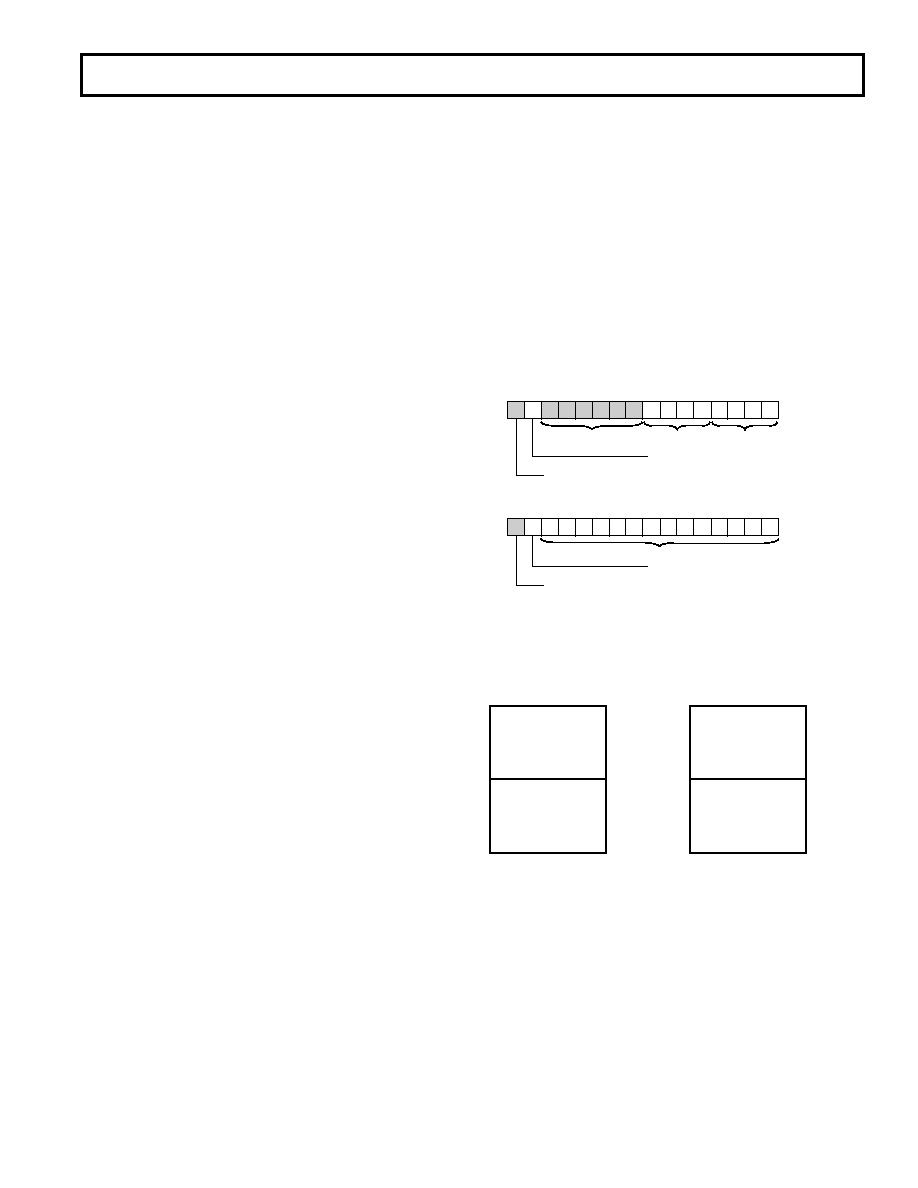
IDMA OVERLAY
DM (0x3FE7)
RESERVED SET TO 0
IDDMOVLAY
IDPMOVLAY
0
0000
0
15 14 13 12 11 10
9
8
7
6
5
43210
SHORT READ ONLY
0 = ENABLE
1 = DISABLE
IDMA CONTROL (U = UNDEFINED AT RESET)
DM (0x3FE0)
IDMAA ADDRESS
U
UUUU
UUUUU
U
15 14 13 12 11 10
9
8
7
6
5
43210
IDMAD DESTINATION MEMORY TYPE
0 = PM
1 = DM
NOTES: RESERVED BITS ARE SHOWN ON A GRAY FIELD. THESE BITS
SHOULD ALWAYS BE WRITTEN WITH ZEROS.
0
RESERVED SET TO 0
0
RESERVED SET TO 0
Figure 10. IDMA Control/OVLAY Registers
ACCESSIBLE WHEN
PMOVLAY = 0
0
x2000 –
0
x3FFF
DMA
PROGRAM MEMORY
OVLAY
ALWAYS
ACCESSIBLE
AT ADDRESS
0
x0000 – 0x1FFF
ACCESSIBLE WHEN
DMOVLAY = 0
0
x0000 –
0
x1FFF
DMA
DATA MEMORY
OVLAY
ALWAYS
ACCESSIBLE
AT ADDRESS
0
x2000 – 0x3FFF
NOTE: IDMA AND BDMA HAVE SEPARATE DMA CONTROL REGISTERS.
Figure 11. Direct Memory Access—PM and DM
Memory Maps
Bootstrap Loading (Booting)
The ADSP-2185M has two mechanisms to allow automatic load-
ing of the internal program memory after reset. The method for
booting is controlled by the Mode A, B, and C configuration bits.
When the MODE pins specify BDMA booting, the ADSP-2185M
initiates a BDMA boot sequence when reset is released.
The BDMA interface is set up during reset to the following
defaults when BDMA booting is specified: the BDIR, BMPAGE,
BIAD, and BEAD registers are set to 0, the BTYPE register is
set to 0 to specify program memory 24-bit words, and the
BWCOUNT register is set to 32. This causes 32 words of
on-chip program memory to be loaded from byte memory.
相关PDF资料 |
PDF描述 |
|---|---|
| VI-23X-CY-F1 | CONVERTER MOD DC/DC 5.2V 50W |
| MAX6519UKP095+T | IC TEMP SENSOR SW SOT23-5 |
| VI-23W-CY-F3 | CONVERTER MOD DC/DC 5.5V 50W |
| VI-23V-CY-F3 | CONVERTER MOD DC/DC 5.8V 50W |
| VE-B6X-EU-B1 | CONVERTER MOD DC/DC 5.2V 200W |
相关代理商/技术参数 |
参数描述 |
|---|---|
| ADSP-2185N | 制造商:AD 制造商全称:Analog Devices 功能描述:DSP Microcomputer |
| ADSP-2185NBCA-320 | 制造商:Analog Devices 功能描述:DSP Fixed-Point 16-Bit 80MHz 80MIPS 144-Pin CSP-BGA 制造商:Rochester Electronics LLC 功能描述:16K PM/16K DM RAM,16-BIT,80 MIPS, 1.8V - Bulk |
| ADSP-2185NBST-320 | 制造商:Analog Devices 功能描述:DSP Fixed-Point 16-Bit 80MHz 80MIPS 100-Pin LQFP 制造商:Analog Devices 功能描述:IC MICROCOMPUTER 16-BIT |
| ADSP-2185NBSTZ-320 | 功能描述:IC DSP CONTROLLER 16BIT 100LQFP RoHS:是 类别:集成电路 (IC) >> 嵌入式 - DSP(数字式信号处理器) 系列:ADSP-21xx 标准包装:2 系列:StarCore 类型:SC140 内核 接口:DSI,以太网,RS-232 时钟速率:400MHz 非易失内存:外部 芯片上RAM:1.436MB 电压 - 输入/输出:3.30V 电压 - 核心:1.20V 工作温度:-40°C ~ 105°C 安装类型:表面贴装 封装/外壳:431-BFBGA,FCBGA 供应商设备封装:431-FCPBGA(20x20) 包装:托盘 |
| ADSP-2185NBSTZ-3202 | 制造商:AD 制造商全称:Analog Devices 功能描述:DSP Microcomputer |
发布紧急采购,3分钟左右您将得到回复。