- 您现在的位置:买卖IC网 > PDF目录19393 > ADSP-2185NBSTZ-320 (Analog Devices Inc)IC DSP CONTROLLER 16BIT 100LQFP PDF资料下载
参数资料
| 型号: | ADSP-2185NBSTZ-320 |
| 厂商: | Analog Devices Inc |
| 文件页数: | 6/48页 |
| 文件大小: | 0K |
| 描述: | IC DSP CONTROLLER 16BIT 100LQFP |
| 标准包装: | 1 |
| 系列: | ADSP-21xx |
| 类型: | 定点 |
| 接口: | 主机接口,串行端口 |
| 时钟速率: | 80MHz |
| 非易失内存: | 外部 |
| 芯片上RAM: | 80kB |
| 电压 - 输入/输出: | 1.8V,2.5V,3.3V |
| 电压 - 核心: | 1.90V |
| 工作温度: | -40°C ~ 85°C |
| 安装类型: | 表面贴装 |
| 封装/外壳: | 100-LQFP |
| 供应商设备封装: | 100-LQFP(14x14) |
| 包装: | 托盘 |
第1页第2页第3页第4页第5页当前第6页第7页第8页第9页第10页第11页第12页第13页第14页第15页第16页第17页第18页第19页第20页第21页第22页第23页第24页第25页第26页第27页第28页第29页第30页第31页第32页第33页第34页第35页第36页第37页第38页第39页第40页第41页第42页第43页第44页第45页第46页第47页第48页
Rev. A
|
Page 14 of 48
|
August 2006
ADSP-218xN
The IDMA port has a 16-bit multiplexed address and data bus
and supports 24-bit program memory. The IDMA port is com-
pletely asynchronous and can be written while the ADSP-218xN
is operating at full speed.
The DSP memory address is latched and then automatically
incremented after each IDMA transaction. An external device
can therefore access a block of sequentially addressed memory
by specifying only the starting address of the block. This
increases throughput as the address does not have to be sent for
each memory access.
IDMA port access occurs in two phases. The first is the IDMA
Address Latch cycle. When the acknowledge is asserted, a 14-bit
address and 1-bit destination type can be driven onto the bus by
an external device. The address specifies an on-chip memory
location, the destination type specifies whether it is a DM or PM
access. The falling edge of the IDMA address latch signal (IAL)
or the missing edge of the IDMA select signal (IS) latches this
value into the IDMAA register.
Once the address is stored, data can be read from, or written to,
the ADSP-218xN’s on-chip memory. Asserting the select line
(IS) and the appropriate read or write line (IRD and IWR
respectively) signals the ADSP-218xN that a particular transac-
tion is required. In either case, there is a one-processor-cycle
delay for synchronization. The memory access consumes one
additional processor cycle.
Once an access has occurred, the latched address is automati-
cally incremented, and another access can occur.
Through the IDMAA register, the DSP can also specify the
starting address and data format for DMA operation.
Asserting the IDMA port select (IS) and address latch enable
(IAL) directs the ADSP-218xN to write the address onto the
IAD14–0 bus into the IDMA Control Register (Figure 14). If Bit
15 is set to 0, IDMA latches the address. If Bit 15 is set to 1,
IDMA latches into the OVLAY register. This register, also
shown in Figure 14, is memory-mapped at address DM
(0x3FE0). Note that the latched address (IDMAA) cannot be
read back by the host.
When Bit 14 in 0x3FE7 is set to zero, short reads use the timing
shown in Figure 36 on Page 38. When Bit 14 in 0x3FE7 is set to
1, timing in Figure 37 on Page 39 applies for short reads in short
read only mode. Set IDDMOVLAY and IDPMOVLAY bits in
the IDMA overlay register as indicated in Table 8. Refer to the
ADSP-218x DSP Hardware Reference for additional details.
Note
: In full memory mode all locations of 4M-byte memory
space are directly addressable. In host memory mode, only
address pin A0 is available, requiring additional external logic to
provide address information for the byte.
Bootstrap Loading (Booting)
ADSP-218xN series members have two mechanisms to allow
automatic loading of the internal program memory after reset.
The method for booting is controlled by the Mode A, B, and C
configuration bits.
When the mode pins specify BDMA booting, the ADSP-218xN
initiates a BDMA boot sequence when reset is released.
The BDMA interface is set up during reset to the following
defaults when BDMA booting is specified: the BDIR, BMPAGE,
BIAD, and BEAD registers are set to 0, the BTYPE register is set
to 0 to specify program memory 24-bit words, and the
BWCOUNT register is set to 32. This causes 32 words of on-
chip program memory to be loaded from byte memory. These
32 words are used to set up the BDMA to load in the remaining
program code. The BCR bit is also set to 1, which causes pro-
gram execution to be held off until all 32 words are loaded into
on-chip program memory. Execution then begins at address 0.
The ADSP-2100 Family development software (Revision 5.02
and later) fully supports the BDMA booting feature and can
generate byte memory space-compatible boot code.
The IDLE instruction can also be used to allow the processor to
hold off execution while booting continues through the BDMA
interface. For BDMA accesses while in Host Mode, the addres-
ses to boot memory must be constructed externally to the
ADSP-218xN. The only memory address bit provided by the
processor is A0.
IDMA Port Booting
ADSP-218xN series members can also boot programs through
its internal DMA port. If Mode C = 1, Mode B = 0, and Mode A
= 1, the ADSP-218xN boots from the IDMA port. IDMA feature
can load as much on-chip memory as desired. Program execu-
tion is held off until the host writes to on-chip program memory
location 0.
BUS REQUEST AND BUS GRANT
ADSP-218xN series members can relinquish control of the data
and address buses to an external device. When the external
device requires access to memory, it asserts the Bus Request
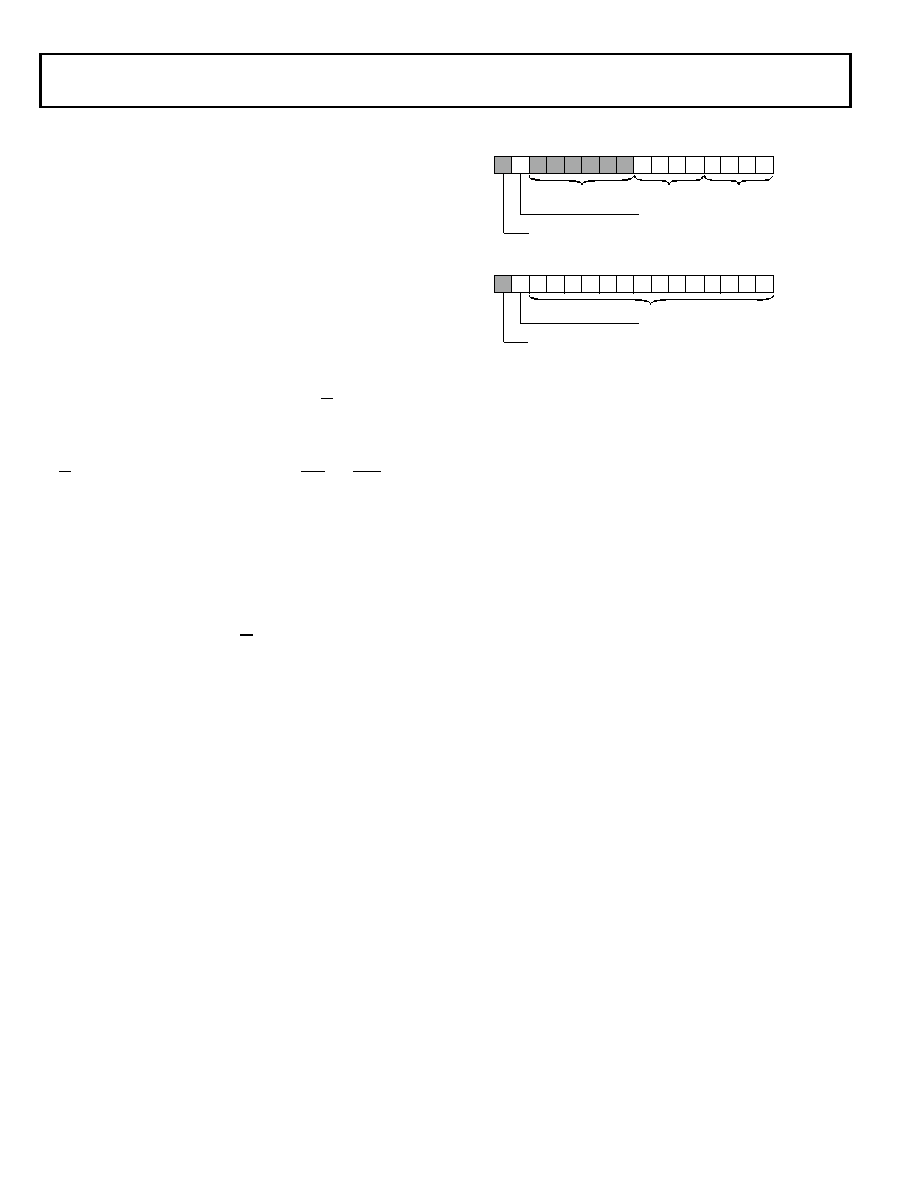
Figure 14. IDMA OVLAY/Control Registers
IDMA OVERLAY
DM (0x3FE7)
RESERVED SET TO 0
IDDMOVLAY
IDPMOVLAY
00
0
00
0
00
0
15 14 1 3 12 11 10
9
8
7
6
5
4
3
2
1
0
SHORT READ
ONLY
0 = DISABLE
1 = ENABLE
IDMA CONTROL (U = UNDEFINED AT RESET)
DM (0x3FE0)
IDMAA ADDRESS
U
UUU
U
UU
U
15 14 13 1 2 11 1 0
9
8
7
6
5
4
3
2
1
0
IDMAD DESTINATION MEMORY
TYPE
0= PM
1= DM
NOTE: RESERVED BITS ARE SHOWN ON A GRAY FIELD. THESE
BITS SHOULD ALWAYS BE WRITTEN WITH ZEROS.
0
RESERVED SET TO 0
0
RESERVED SET TO 0
(SEE TABLE 12)
相关PDF资料 |
PDF描述 |
|---|---|
| EBM08DSXN | CONN EDGECARD 16POS DIP .156 SLD |
| RMC35DRXI-S734 | CONN EDGECARD 70POS DIP .100 SLD |
| EBM08DSXH | CONN EDGECARD 16POS DIP .156 SLD |
| HMC31DRXN-S734 | CONN EDGECARD 62POS DIP .100 SLD |
| EEM06DSEI | CONN EDGECARD 12POS .156 EYELET |
相关代理商/技术参数 |
参数描述 |
|---|---|
| ADSP-2185NBSTZ-3202 | 制造商:AD 制造商全称:Analog Devices 功能描述:DSP Microcomputer |
| ADSP-2185NKCA-320 | 功能描述:IC DSP 16BIT 80MHZ 144CSPBGA RoHS:否 类别:集成电路 (IC) >> 嵌入式 - DSP(数字式信号处理器) 系列:ADSP-21xx 标准包装:2 系列:StarCore 类型:SC140 内核 接口:DSI,以太网,RS-232 时钟速率:400MHz 非易失内存:外部 芯片上RAM:1.436MB 电压 - 输入/输出:3.30V 电压 - 核心:1.20V 工作温度:-40°C ~ 105°C 安装类型:表面贴装 封装/外壳:431-BFBGA,FCBGA 供应商设备封装:431-FCPBGA(20x20) 包装:托盘 |
| ADSP-2185NKCAZ-320 | 功能描述:IC DSP 16BIT 80MHZ 144CSPBGA RoHS:是 类别:集成电路 (IC) >> 嵌入式 - DSP(数字式信号处理器) 系列:ADSP-21xx 标准包装:2 系列:StarCore 类型:SC140 内核 接口:DSI,以太网,RS-232 时钟速率:400MHz 非易失内存:外部 芯片上RAM:1.436MB 电压 - 输入/输出:3.30V 电压 - 核心:1.20V 工作温度:-40°C ~ 105°C 安装类型:表面贴装 封装/外壳:431-BFBGA,FCBGA 供应商设备封装:431-FCPBGA(20x20) 包装:托盘 |
| ADSP-2185NKST-320 | 制造商:Analog Devices 功能描述:DSP Fixed-Point 16-Bit 80MHz 80MIPS 100-Pin LQFP 制造商:Rochester Electronics LLC 功能描述:16K PM/16K DM RAM,16-BIT, 80 MIPS, 1.8V - Bulk 制造商:Analog Devices 功能描述:Digital Signal Processor IC Supply Volta |
| ADSP-2185NKSTZ-320 | 功能描述:IC DSP CONTROLLER 16BIT 100LQFP RoHS:是 类别:集成电路 (IC) >> 嵌入式 - DSP(数字式信号处理器) 系列:ADSP-21xx 标准包装:40 系列:TMS320DM64x, DaVinci™ 类型:定点 接口:I²C,McASP,McBSP 时钟速率:400MHz 非易失内存:外部 芯片上RAM:160kB 电压 - 输入/输出:3.30V 电压 - 核心:1.20V 工作温度:0°C ~ 90°C 安装类型:表面贴装 封装/外壳:548-BBGA,FCBGA 供应商设备封装:548-FCBGA(27x27) 包装:托盘 配用:TMDSDMK642-0E-ND - DEVELPER KIT W/NTSC CAMERA296-23038-ND - DSP STARTER KIT FOR TMS320C6416296-23059-ND - FLASHBURN PORTING KIT296-23058-ND - EVAL MODULE FOR DM642TMDSDMK642-ND - DEVELOPER KIT W/NTSC CAMERA |
发布紧急采购,3分钟左右您将得到回复。