- 您现在的位置:买卖IC网 > PDF目录19397 > ADSP-2186MKSTZ-300 (Analog Devices Inc)IC DSP CONTROLLER 16BIT 100LQFP PDF资料下载
参数资料
| 型号: | ADSP-2186MKSTZ-300 |
| 厂商: | Analog Devices Inc |
| 文件页数: | 5/40页 |
| 文件大小: | 0K |
| 描述: | IC DSP CONTROLLER 16BIT 100LQFP |
| 标准包装: | 1 |
| 系列: | ADSP-21xx |
| 类型: | 定点 |
| 接口: | 主机接口,串行端口 |
| 时钟速率: | 75MHz |
| 非易失内存: | 外部 |
| 芯片上RAM: | 40kB |
| 电压 - 输入/输出: | 3.30V |
| 电压 - 核心: | 2.50V |
| 工作温度: | 0°C ~ 70°C |
| 安装类型: | 表面贴装 |
| 封装/外壳: | 100-LQFP |
| 供应商设备封装: | 100-LQFP(14x14) |
| 包装: | 托盘 |
第1页第2页第3页第4页当前第5页第6页第7页第8页第9页第10页第11页第12页第13页第14页第15页第16页第17页第18页第19页第20页第21页第22页第23页第24页第25页第26页第27页第28页第29页第30页第31页第32页第33页第34页第35页第36页第37页第38页第39页第40页
REV. 0
ADSP-2186M
–13–
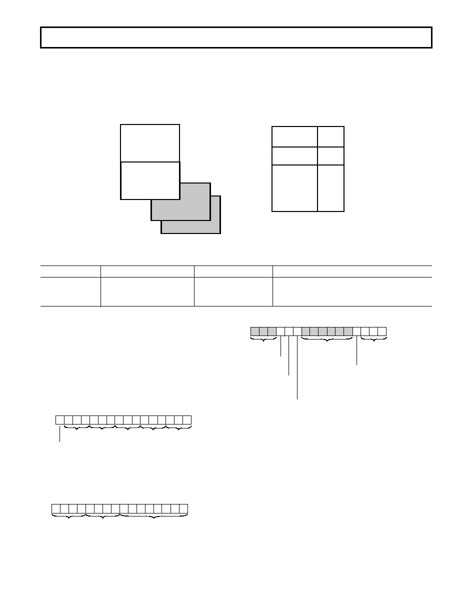
Data Memory
Data Memory (Full Memory Mode) is a 16-bit-wide space used
for the storage of data variables and for memory-mapped control
registers. The ADSP-2186M has 8K words on Data Memory
RAM on-chip. Part of this space is used by 32 memory-mapped
registers. Support also exists for up to two 8K external memory
overlay spaces through the external data bus. All internal accesses
ACCESSIBLE WHEN
DMOVLAY = 2
ACCESSIBLE WHEN
DMOVLAY = 1
0x0000 – 0x1FFF1
EXTERNAL
MEMORY
32 MEMORY
MAPPED
REGISTERS
0x3FFF
INTERNAL
8160 WORDS
0x0000
DATA MEMORY
ADDR
0x3FE0
EXTERNAL 8K
DMOVLAY = 1, 2
0x1FFF
0x3FDF
0x2000
DM OVLAY = 0
RESERVED
0x0000 – 0x1FFF
DATA MEMORY
ALWAYS
ACCESSIBLE
AT ADDRESS
0x2000 – 0x3FFF
NOTE:
1SEE TABLE IV FOR DMOVLAY BITS
Figure 5. Data Memory Map
complete in one cycle. Accesses to external memory are timed
using the wait states specified by the DWAIT register and the
wait state mode bit.
Data Memory (Host Mode) allows access to all internal
memory. External overlay access is limited by a single external
address line (A0).
Table IV. DMOVLAY Bits
DMOVLAY
Memory
A13
A12:0
0
Reserved
Not Applicable
1
External Overlay 1
0
13 LSBs of Address Between 0x2000 and 0x3FFF
2
External Overlay 2
1
13 LSBs of Address Between 0x2000 and 0x3FFF
Memory Mapped Registers (New to the ADSP-2186M)
The ADSP-2186M has three memory mapped registers that differ
from other ADSP-21xx Family DSPs. The slight modifications
to these registers (Wait State Control, Programmable Flag and
Composite Select Control, and System Control) provide the
ADSP-2186M’s wait state and
BMS control features. Default
bit values at reset are shown; if no value is shown, the bit is unde-
fined at reset. Reserved bits are shown on a grey field. These bits
should always be written with zeros.
DWAIT
IOWAIT3
IOWAIT2
IOWAIT1
IOWAIT0
DM(0x3FFE)
WAITSTATE CONTROL
11
1
11
111
1
15 14 13 12 11 10
9
8
7
6
5
43210
WAIT STATE MODE SELECT
0 = NORMAL MODE (PWAIT, DWAIT, IOWAIT0–3 = N WAIT STATES, RANGING
FROM 0 TO 7)
1 = 2N + 1 MODE (PWAIT, DWAIT, IOWAIT0–3 = 2N + 1 WAIT STATES, RANGING
FROM 0 TO 15)
Figure 6. Wait State Control Register
BMWAIT
CMSSEL
0 = DISABLE
CMS
1 = ENABLE
CMS
DM(0x3FE6)
PROGRAMMABLE FLAG AND COMPOSITE SELECT CONTROL
PFTYPE
0 = INPUT
1 = OUTPUT
(WHERE BIT: 11-IOM, 10-BM, 9-DM, 8-PM)
11
1
0
11
000
0
15 14 13 12 11 10
9
8
7
6
5
43210
Figure 7. Programmable Flag and Composite Control
Register
RESERVED, ALWAYS
SET TO 0
SPORT0 ENABLE
0 = DISABLE
1 = ENABLE
DM(0x3FFF)
SYSTEM CONTROL
SPORT1 ENABLE
0 = DISABLE
1 = ENABLE
SPORT1 CONFIGURE
0 = FI, FO,
IRQ0, IRQ1, SCLK
1 = SPORT1
DISABLE
BMS
0 = ENABLE
BMS
1 = DISABLE
BMS, EXCEPT WHEN MEMORY
STROBES ARE THREE-STATED
PWAIT
PROGRAM MEMORY
WAIT STATES
00
0
1
00
000
0
1
15 14 13 12 11 10
9
8
7
6
5
43210
NOTE: RESERVED BITS ARE SHOWN ON A GRAY FIELD. THESE BITS SHOULD
ALWAYS BE WRITTEN WITH ZEROS.
RESERVED
SET TO 0
Figure 8. System Control Register
I/O Space (Full Memory Mode)
The ADSP-2186M supports an additional external memory
space called I/O space. This space is designed to support simple
connections to peripherals (such as data converters and external
registers) or to bus interface ASIC data registers. I/O space sup-
ports 2048 locations of 16-bit wide data. The lower eleven bits
of the external address bus are used; the upper three bits are
undefined. Two instructions were added to the core ADSP-2100
Family instruction set to read from and write to I/O memory
space. The I/O space also has four dedicated three-bit wait state
registers, IOWAIT0–3, which in combination with the wait state
mode bit, specify up to 15 wait states to be automatically gener-
ated for each of four regions. The wait states act on address
ranges as shown in Table V.
相关PDF资料 |
PDF描述 |
|---|---|
| RW2-0515D/SMD | CONV DC/DC 2W 4.5-9VIN +/-15VOUT |
| VI-B6P-EU-B1 | CONVERTER MOD DC/DC 13.8V 200W |
| MLP2520S1R0S | INDUCTOR MULTILAYER 1.0UH 1008 |
| TPSC476M016S0110 | CAP TANT 47UF 16V 20% 2312 |
| HSC28DRAI-S734 | CONN EDGECARD 56POS .100 R/A PCB |
相关代理商/技术参数 |
参数描述 |
|---|---|
| ADSP-2186MKSTZ300R | 功能描述:IC DSP CONTROLLER 16BIT 100LQFP RoHS:是 类别:集成电路 (IC) >> 嵌入式 - DSP(数字式信号处理器) 系列:ADSP-21xx 标准包装:2 系列:StarCore 类型:SC140 内核 接口:DSI,以太网,RS-232 时钟速率:400MHz 非易失内存:外部 芯片上RAM:1.436MB 电压 - 输入/输出:3.30V 电压 - 核心:1.20V 工作温度:-40°C ~ 105°C 安装类型:表面贴装 封装/外壳:431-BFBGA,FCBGA 供应商设备封装:431-FCPBGA(20x20) 包装:托盘 |
| ADSP-2186N | 制造商:未知厂家 制造商全称:未知厂家 功能描述:ADSP-2184N-ADSP-2189N: DSP Microcomputer Data Sheet (Rev. 0. 10/01) |
| ADSP-2186NBCA-320 | 制造商:Analog Devices 功能描述:DSP Fixed-Point 16-Bit 80MHz 80MIPS 144-Pin CSP-BGA 制造商:Rochester Electronics LLC 功能描述:8K PM/8K DM RAM,16-BIT,80 MIPS, 1.8V - Bulk |
| ADSP-2186NBST-320 | 制造商:Analog Devices 功能描述:DSP Fixed-Point 16-Bit 80MHz 80MIPS 100-Pin LQFP 制造商:Rochester Electronics LLC 功能描述:8K PM/8K DM RAM,16-BIT, 80 MIPS, 1.8V - Bulk 制造商:Analog Devices 功能描述:IC MICROCOMPUTER 16-BIT |
| ADSP-2186NBSTZ-320 | 功能描述:IC DSP CONTROLLER 16BIT 100LQFP RoHS:是 类别:集成电路 (IC) >> 嵌入式 - DSP(数字式信号处理器) 系列:ADSP-21xx 标准包装:40 系列:TMS320DM64x, DaVinci™ 类型:定点 接口:I²C,McASP,McBSP 时钟速率:400MHz 非易失内存:外部 芯片上RAM:160kB 电压 - 输入/输出:3.30V 电压 - 核心:1.20V 工作温度:0°C ~ 90°C 安装类型:表面贴装 封装/外壳:548-BBGA,FCBGA 供应商设备封装:548-FCBGA(27x27) 包装:托盘 配用:TMDSDMK642-0E-ND - DEVELPER KIT W/NTSC CAMERA296-23038-ND - DSP STARTER KIT FOR TMS320C6416296-23059-ND - FLASHBURN PORTING KIT296-23058-ND - EVAL MODULE FOR DM642TMDSDMK642-ND - DEVELOPER KIT W/NTSC CAMERA |
发布紧急采购,3分钟左右您将得到回复。