- 您现在的位置:买卖IC网 > PDF目录19405 > ADSP-2186MKSTZ300R (Analog Devices Inc)IC DSP CONTROLLER 16BIT 100LQFP PDF资料下载
参数资料
| 型号: | ADSP-2186MKSTZ300R |
| 厂商: | Analog Devices Inc |
| 文件页数: | 2/40页 |
| 文件大小: | 0K |
| 描述: | IC DSP CONTROLLER 16BIT 100LQFP |
| 标准包装: | 1 |
| 系列: | ADSP-21xx |
| 类型: | 定点 |
| 接口: | 主机接口,串行端口 |
| 时钟速率: | 75MHz |
| 非易失内存: | 外部 |
| 芯片上RAM: | 40kB |
| 电压 - 输入/输出: | 3.30V |
| 电压 - 核心: | 2.50V |
| 工作温度: | 0°C ~ 70°C |
| 安装类型: | 表面贴装 |
| 封装/外壳: | 100-LQFP |
| 供应商设备封装: | 100-LQFP(14x14) |
| 包装: | 标准包装 |
| 其它名称: | ADSP-2186MKSTZ300RDKR |
第1页当前第2页第3页第4页第5页第6页第7页第8页第9页第10页第11页第12页第13页第14页第15页第16页第17页第18页第19页第20页第21页第22页第23页第24页第25页第26页第27页第28页第29页第30页第31页第32页第33页第34页第35页第36页第37页第38页第39页第40页
REV. 0
–10–
ADSP-2186M
Slow Idle
The IDLE instruction is enhanced on the ADSP-2186M to let
the processor’s internal clock signal be slowed, further reducing
power consumption. The reduced clock frequency, a program-
mable fraction of the normal clock rate, is specified by a selectable
divisor given in the IDLE instruction.
The format of the instruction is:
IDLE (n);
where n = 16, 32, 64, or 128. This instruction keeps the proces-
sor fully functional, but operating at the slower clock rate. While
it is in this state, the processor’s other internal clock signals, such
as SCLK, CLKOUT, and timer clock, are reduced by the same
ratio. The default form of the instruction, when no clock divisor
is given, is the standard IDLE instruction.
When the IDLE (n) instruction is used, it effectively slows down
the processor’s internal clock and thus its response time to incom-
ing interrupts. The one-cycle response time of the standard idle
state is increased by n, the clock divisor. When an enabled inter-
rupt is received, the ADSP-2186M will remain in the idle state
for up to a maximum of n processor cycles (n = 16, 32, 64, or
128) before resuming normal operation.
When the IDLE (n) instruction is used in systems that have an
externally generated serial clock (SCLK), the serial clock rate
may be faster than the processor’s reduced internal clock rate.
Under these conditions, interrupts must not be generated at a
faster than can be serviced, due to the additional time the
processor takes to come out of the idle state (a maximum of n
processor cycles).
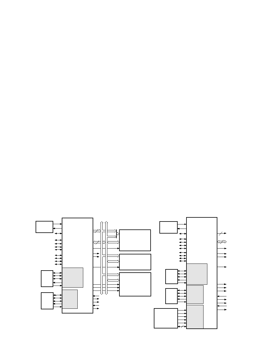
SYSTEM INTERFACE
Figure 2 shows typical basic system configurations with the
ADSP-2186M, two serial devices, a byte-wide EPROM, and
optional external program and data overlay memories (mode-
selectable). Programmable wait state generation allows the
processor to connect easily to slow peripheral devices. The
ADSP-2186M also provides four external interrupts and two
serial ports or six external interrupts and one serial port. Host
Memory Mode allows access to the full external data bus, but
limits addressing to a single address bit (A0). Through the use
of external hardware, additional system peripherals can be added
in this mode to generate and latch address signals.
Clock Signals
The ADSP-2186M can be clocked by either a crystal or a
TTL-compatible clock signal.
The CLKIN input cannot be halted, changed during opera-
tion, nor operated below the specified frequency during normal
operation. The only exception is while the processor is in the
power-down state. For additional information, refer to Chap-
ter 9, ADSP-2100 Family User’s Manual, for detailed information
on this power-down feature.
If an external clock is used, it should be a TTL-compatible signal
running at half the instruction rate. The signal is connected to
the processor’s CLKIN input. When an external clock is used,
the XTAL input must be left unconnected.
The ADSP-2186M uses an input clock with a frequency equal to
half the instruction rate; a 37.50 MHz input clock yields a 13 ns
processor cycle (which is equivalent to 75 MHz). Normally,
instructions are executed in a single processor cycle. All device
timing is relative to the internal instruction clock rate, which is
indicated by the CLKOUT signal when enabled.
Because the ADSP-2186M includes an on-chip oscillator circuit,
an external crystal may be used. The crystal should be connected
across the CLKIN and XTAL pins, with two capacitors con-
nected as shown in Figure 3. Capacitor values are dependent on
crystal type and should be specified by the crystal manufacturer.
A parallel-resonant, fundamental frequency, microprocessor-
grade crystal should be used.
A clock output (CLKOUT) signal is generated by the processor
at the processor’s cycle rate. This can be enabled and disabled by
the CLKODIS bit in the SPORT0 Autobuffer Control Register.
1/2x CLOCK
OR
CRYSTAL
FL0–2
CLKIN
XTAL
SERIAL
DEVICE
SCLK1
RFS1 OR
IRQ0
TFS1 OR
IRQ1
DT1 OR FO
DR1 OR FI
SPORT1
SERIAL
DEVICE
A0–A21
DATA
BYTE
MEMORY
I/O SPACE
(PERIPHERALS)
DATA
ADDR
DATA
ADDR
2048 LOCATIONS
OVERLAY
MEMORY
TWO 8K
PM SEGMENTS
TWO 8K
DM SEGMENTS
D23–0
A13–0
D23–8
A10–0
D15–8
D23–16
A13–0
14
24
SCLK0
RFS0
TFS0
DT0
DR0
SPORT0
ADDR13–0
DATA23–0
ADSP-2186M
CS
1/2x CLOCK
OR
CRYSTAL
SERIAL
DEVICE
SPORT1
16
IDMA PORT
SERIAL
DEVICE
SPORT0
1
16
ADSP-2186M
HOST MEMORY MODE
FULL MEMORY MODE
MODE D/PF3
MODE C/PF2
MODE B/PF1
MODE A/PF0
SYSTEM
INTERFACE
OR
CONTROLLER
IRQ2/PF7
IRQE/PF4
IRQL0/PF5
IRQL1/PF6
IOMS
BMS
PMS
DMS
CMS
BR
BG
BGH
PWD
PWDACK
WR
RD
ADSP-2186M
CLKIN
XTAL
FL0–2
SCLK1
RFS1 OR
IRQ0
TFS1 OR
IRQ1
DT1 OR FO
DR1 OR FI
IRD/D6
IWR/D7
IS/D4
IAL/D5
IACK/D3
IAD15–0
SCLK0
RFS0
TFS0
DT0
DR0
IRQ2/PF7
IRQE/PF4
IRQL0/PF5
IRQL1/PF6
MODE D/PF3
MODE C/PF2
MODE B/PF1
MODE A/PF0
A0
DATA23–8
IOMS
BMS
PMS
DMS
CMS
BR
BG
BGH
PWD
PWDACK
WR
RD
Figure 2. Basic System Interface
相关PDF资料 |
PDF描述 |
|---|---|
| MAX6501UKP055+T | IC TEMP SWITCH SOT23-5 |
| GMA50DTBN | CONN EDGECARD 100PS R/A .125 SLD |
| TPSB336K010A0650 | CAP TANT 33UF 10V 10% 1210 |
| GBC18DCMI-S288 | CONN EDGECARD 36POS .100 EXTEND |
| TMS320C6416TBZLZ1 | IC FIXED-POINT DSP 532-FCBGA |
相关代理商/技术参数 |
参数描述 |
|---|---|
| ADSP-2186N | 制造商:未知厂家 制造商全称:未知厂家 功能描述:ADSP-2184N-ADSP-2189N: DSP Microcomputer Data Sheet (Rev. 0. 10/01) |
| ADSP-2186NBCA-320 | 制造商:Analog Devices 功能描述:DSP Fixed-Point 16-Bit 80MHz 80MIPS 144-Pin CSP-BGA 制造商:Rochester Electronics LLC 功能描述:8K PM/8K DM RAM,16-BIT,80 MIPS, 1.8V - Bulk |
| ADSP-2186NBST-320 | 制造商:Analog Devices 功能描述:DSP Fixed-Point 16-Bit 80MHz 80MIPS 100-Pin LQFP 制造商:Rochester Electronics LLC 功能描述:8K PM/8K DM RAM,16-BIT, 80 MIPS, 1.8V - Bulk 制造商:Analog Devices 功能描述:IC MICROCOMPUTER 16-BIT |
| ADSP-2186NBSTZ-320 | 功能描述:IC DSP CONTROLLER 16BIT 100LQFP RoHS:是 类别:集成电路 (IC) >> 嵌入式 - DSP(数字式信号处理器) 系列:ADSP-21xx 标准包装:40 系列:TMS320DM64x, DaVinci™ 类型:定点 接口:I²C,McASP,McBSP 时钟速率:400MHz 非易失内存:外部 芯片上RAM:160kB 电压 - 输入/输出:3.30V 电压 - 核心:1.20V 工作温度:0°C ~ 90°C 安装类型:表面贴装 封装/外壳:548-BBGA,FCBGA 供应商设备封装:548-FCBGA(27x27) 包装:托盘 配用:TMDSDMK642-0E-ND - DEVELPER KIT W/NTSC CAMERA296-23038-ND - DSP STARTER KIT FOR TMS320C6416296-23059-ND - FLASHBURN PORTING KIT296-23058-ND - EVAL MODULE FOR DM642TMDSDMK642-ND - DEVELOPER KIT W/NTSC CAMERA |
| ADSP-2186NBSTZ-3202 | 制造商:AD 制造商全称:Analog Devices 功能描述:DSP Microcomputer |
发布紧急采购,3分钟左右您将得到回复。