- 您现在的位置:买卖IC网 > PDF目录19481 > ADSP-BF506BSWZ-4F (Analog Devices Inc)IC DSP 400MHZ 1.4V 120LQFP PDF资料下载
参数资料
| 型号: | ADSP-BF506BSWZ-4F |
| 厂商: | Analog Devices Inc |
| 文件页数: | 47/80页 |
| 文件大小: | 0K |
| 描述: | IC DSP 400MHZ 1.4V 120LQFP |
| 视频文件: | Blackfin? BF50x Processor Family |
| 标准包装: | 1 |
| 系列: | Blackfin® |
| 类型: | 定点 |
| 接口: | CAN,EBI/EMI,I²C,IrDA,PPI,SPI,SPORT,UART/USART |
| 时钟速率: | 400MHz |
| 非易失内存: | 闪存(16MB) |
| 芯片上RAM: | 68kB |
| 电压 - 输入/输出: | 3.30V |
| 电压 - 核心: | 1.29V |
| 工作温度: | -40°C ~ 85°C |
| 安装类型: | 表面贴装 |
| 封装/外壳: | 120-LQFP 裸露焊盘 |
| 供应商设备封装: | 120-LQFP-EP(14x14) |
| 包装: | 托盘 |
第1页第2页第3页第4页第5页第6页第7页第8页第9页第10页第11页第12页第13页第14页第15页第16页第17页第18页第19页第20页第21页第22页第23页第24页第25页第26页第27页第28页第29页第30页第31页第32页第33页第34页第35页第36页第37页第38页第39页第40页第41页第42页第43页第44页第45页第46页当前第47页第48页第49页第50页第51页第52页第53页第54页第55页第56页第57页第58页第59页第60页第61页第62页第63页第64页第65页第66页第67页第68页第69页第70页第71页第72页第73页第74页第75页第76页第77页第78页第79页第80页
Rev. A
|
Page 51 of 80
|
July 2011
ADSP-BF504/ADSP-BF504F/ADSP-BF506F
Output Disable Time Measurement
Output pins are considered to be disabled when they stop driv-
ing, go into a high impedance state, and start to decay from their
output high or low voltage. The output disable time t
DIS is the
difference between t
DIS
_MEASURED and tDECAY as shown on the left side
of Figure 42.
The time for the voltage on the bus to decay by
ΔV is dependent
on the capacitive load C
L and the load current IL. This decay time
can be approximated by the equation:
The time t
DECAY is calculated with test loads CL and IL, and with
ΔV equal to 0.25 V for V
DDEXT (nominal) = 2.5 V/3.3 V and
0.15 V for VDDEXT (nominal) = 1.8 V.
The time t
DIS
_MEASURED is the interval from when the reference sig-
nal switches, to when the output voltage decays
ΔV from the
measured output high or output low voltage.
Example System Hold Time Calculation
To determine the data output hold time in a particular system,
first calculate t
DECAY using the equation given above. Choose ΔV
to be the difference between the processor’s output voltage and
the input threshold for the device requiring the hold time. C
L is
the total bus capacitance (per data line), and I
L is the total leak-
age or three-state current (per data line). The hold time will be
t
DECAY plus the various output disable times as specified in the
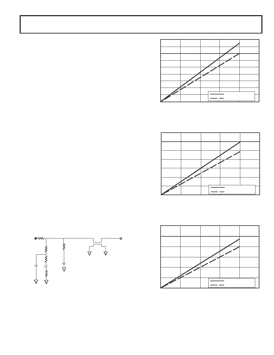
Capacitive Loading
Output delays and holds are based on standard capacitive loads
how output rise time varies with capacitance. The delay and
hold specifications given should be derated by a factor derived
from these figures. The graphs in these figures may not be linear
outside the ranges shown.
Figure 43. Equivalent Device Loading for AC Measurements
(Includes All Fixtures)
tDIS
tDIS_MEASURED tDECAY
–
=
tDECAY
CL V
Δ
() I
L
=
T1
ZO = 50
: (impedance)
TD = 4.04
r 1.18 ns
2pF
TESTER PIN ELECTRONICS
50
:
0.5pF
70
:
400
:
45
:
4pF
NOTES:
THE WORST CASE TRANSMISSION LINE DELAY IS SHOWN AND CAN BE USED
FOR THE OUTPUT TIMING ANALYSIS TO REFELECT THE TRANSMISSION LINE
EFFECT AND MUST BE CONSIDERED. THE TRANSMISSION LINE (TD), IS FOR
LOAD ONLY AND DOES NOT AFFECT THE DATA SHEET TIMING SPECIFICATIONS.
ANALOG DEVICES RECOMMENDS USING THE IBIS MODEL TIMING FOR A GIVEN
SYSTEM REQUIREMENT. IF NECESSARY, A SYSTEM MAY INCORPORATE
EXTERNAL DRIVERS TO COMPENSATE FOR ANY TIMING DIFFERENCES.
VLOAD
DUT
OUTPUT
50
:
Figure 44. Driver Type B Typical Rise and Fall Times (10%–90%) vs.
Load Capacitance (1.8 V VDDEXT)
Figure 45. Driver Type B Typical Rise and Fall Times (10%–90%) vs.
Load Capacitance (2.5 V VDDEXT)
Figure 46. Driver Type B Typical Rise and Fall Times (10%–90%) vs.
Load Capacitance (3.3 V VDDEXT)
4
RISE
AND
F
ALL
TIME
(ns)
LOAD CAPACITANCE (pF)
0
50
100
150
250
9
7
0
1
3
6
200
t
RISE
t
FALL
t
RISE = 1.8V @ 25°C
t
FALL = 1.8V @ 25°C
2
5
8
4
RISE
AND
F
ALL
TIME
(ns)
LOAD CAPACITANCE (pF)
0
50
100
150
250
7
6
0
1
2
5
200
t
RISE
t
FALL
3
t
RISE = 2.5V @ 25°C
t
FALL = 2.5V @ 25°C
3
RISE
AND
F
ALL
TIME
(ns)
LOAD CAPACITANCE (pF)
0
50
100
150
250
6
5
0
1
2
4
200
t
RISE
t
FALL
t
RISE = 3.3V @ 25°C
t
FALL = 3.3V @ 25°C
相关PDF资料 |
PDF描述 |
|---|---|
| GMC60DREH-S734 | CONN EDGECARD 120PS .100 EYELET |
| XC95288XL-10FGG256C | IC CPLD 288MCELL 10NS 256-FBGA |
| HMC05DRXH | CONN EDGECARD 10POS DIP .100 SLD |
| RGM43DRSD-S288 | CONN EDGECARD 86POS .156 EXTEND |
| VE-B5K-CY-F1 | CONVERTER MOD DC/DC 40V 50W |
相关代理商/技术参数 |
参数描述 |
|---|---|
| ADSP-BF506BSWZ-4FX | 制造商:Analog Devices 功能描述:- Trays |
| ADSP-BF506F | 制造商:Analog Devices 功能描述:LOW POWER BLACKFIN WITH ADVANCED EMBEDDED CONNECTIVITY - Bulk |
| ADSPBF506FBSWZ-ENG | 制造商:Analog Devices 功能描述:- Trays |
| ADSP-BF506KSWZ-3F | 功能描述:IC DSP 12BIT 300MHZ 120LQFP RoHS:是 类别:集成电路 (IC) >> 嵌入式 - DSP(数字式信号处理器) 系列:Blackfin® 标准包装:2 系列:StarCore 类型:SC140 内核 接口:DSI,以太网,RS-232 时钟速率:400MHz 非易失内存:外部 芯片上RAM:1.436MB 电压 - 输入/输出:3.30V 电压 - 核心:1.20V 工作温度:-40°C ~ 105°C 安装类型:表面贴装 封装/外壳:431-BFBGA,FCBGA 供应商设备封装:431-FCPBGA(20x20) 包装:托盘 |
| ADSP-BF506KSWZ-4F | 功能描述:IC DSP 12BIT 400MHZ 120LQFP RoHS:是 类别:集成电路 (IC) >> 嵌入式 - DSP(数字式信号处理器) 系列:Blackfin® 标准包装:2 系列:StarCore 类型:SC140 内核 接口:DSI,以太网,RS-232 时钟速率:400MHz 非易失内存:外部 芯片上RAM:1.436MB 电压 - 输入/输出:3.30V 电压 - 核心:1.20V 工作温度:-40°C ~ 105°C 安装类型:表面贴装 封装/外壳:431-BFBGA,FCBGA 供应商设备封装:431-FCPBGA(20x20) 包装:托盘 |
发布紧急采购,3分钟左右您将得到回复。