- 您现在的位置:买卖IC网 > PDF目录19398 > ADSP-BF522KBCZ-4 (Analog Devices Inc)IC DSP CTRLR 400MHZ 289CSPBGA PDF资料下载
参数资料
| 型号: | ADSP-BF522KBCZ-4 |
| 厂商: | Analog Devices Inc |
| 文件页数: | 16/88页 |
| 文件大小: | 0K |
| 描述: | IC DSP CTRLR 400MHZ 289CSPBGA |
| 标准包装: | 1 |
| 系列: | Blackfin® |
| 类型: | 定点 |
| 接口: | DMA,I²C,PPI,SPI,SPORT,UART |
| 时钟速率: | 400MHz |
| 非易失内存: | ROM(32 kB) |
| 芯片上RAM: | 132kB |
| 电压 - 输入/输出: | 1.8V,2.5V,3.3V |
| 电压 - 核心: | 1.30V |
| 工作温度: | 0°C ~ 70°C |
| 安装类型: | 表面贴装 |
| 封装/外壳: | 289-LFBGA,CSPBGA |
| 供应商设备封装: | 289-CSPBGA(12x12) |
| 包装: | 托盘 |
第1页第2页第3页第4页第5页第6页第7页第8页第9页第10页第11页第12页第13页第14页第15页当前第16页第17页第18页第19页第20页第21页第22页第23页第24页第25页第26页第27页第28页第29页第30页第31页第32页第33页第34页第35页第36页第37页第38页第39页第40页第41页第42页第43页第44页第45页第46页第47页第48页第49页第50页第51页第52页第53页第54页第55页第56页第57页第58页第59页第60页第61页第62页第63页第64页第65页第66页第67页第68页第69页第70页第71页第72页第73页第74页第75页第76页第77页第78页第79页第80页第81页第82页第83页第84页第85页第86页第87页第88页
�� �
�
�ADSP-BF522/ADSP-BF523/ADSP-BF524/ADSP-BF525/ADSP-BF526/ADSP-BF527�
�ADSP-BF523/ADSP-BF525/ADSP-BF527�
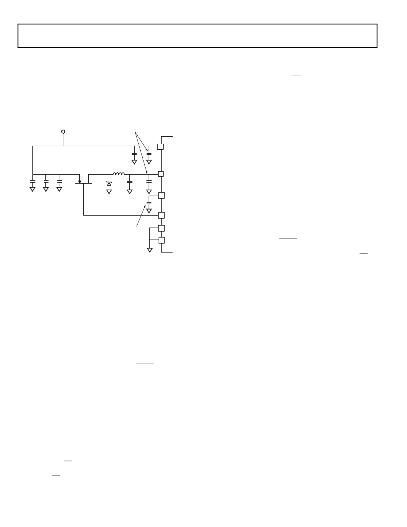
�VOLTAGE� REGULATION�
�The� ADSP-BF523/ADSP-BF525/ADSP-BF527� provides� an� on-�
�chip� voltage� regulator� that� can� generate� processor� core� voltage�
�levels� from� an� external� supply.� Figure� 5� shows� the� typical� exter-�
�nal� components� required� to� complete� the� power� management�
�system.�
�regulator,� it� is� Power� Good.� The� Soft� Start� feature� is� recom-�
�mended� to� reduce� the� inrush� currents� and� to� reduce� V� DDINT�
�voltage� overshoot� when� coming� o� ut� of� hibernate� or� changing�
�voltage� levels.� The� Power� Good� (PG)� input� signal� allows� the�
�processor� to� start� only� after� the� internal� voltage� has� reached� a�
�chosen� level.� In� this� way,� the� startup� time� of� the� external�
�regulator� is� detected� after� hibernation.� For� a� complete�
�description� of� Soft� Start� and� Power� Good� functionality,� refer�
�to� the� ADSP-BF52x� Blackfin� Processor� Hardware� Reference� .�
�2.25V� TO� 3.6V�
�INPUT� VOLTAGE�
�RANGE�
�V� DDEXT�
�(LOW-INDUCTANCE)�
�SET� OF� DECOUPLING�
�CAPACITORS�
�ADSP-BF522/ADSP-BF524/ADSP-BF526�
�VOLTAGE� REGULATION�
�100μF�
�+�
�V� DDEXT�
�The� ADSP-BF522/ADSP-BF524/ADSP-BF526� processor�
�requires� an� external� voltage� regulator� to� power� the� V� DDINT�
�domain.� To� reduce� standby� power� consumption,� the� external�
�100μF�
�+�
�10μ� F�
�LOW� ESR�
�100nF�
�FDS9431A�
�10μH�
�ZHCS1000�
�+�
�100μF�
�V� DDINT�
�SS/� PG�
�voltage� regulator� can� be� signaled� through� EXT_WAKE0� or�
�EXT_WAKE1� to� remove� power� from� the� processor� core.� These�
�identical� signals� are� high-true� for� power-up� and� may� be� con-�
�nected� directly� to� the� low-true� shut� down� input� of� many�
�common� regulators.� While� in� the� hibernate� state,� all� external�
�supplies� (V� DDEXT� ,� V� DDMEM� ,� V� DDUSB� ,� V� DDOTP� )� can� still� be� applied,�
�SHORT� AND� LOW-�
�INDUCTANCE� WIRE�
�SEE� H/W� REFERENCE,�
�SYSTEM� DESIGN� CHAPTER,�
�TO� DETERMINE� VALUE�
�VR� OUT�
�EXT_WAKE1�
�VR� SEL�
�eliminating� the� need� for� external� buffers.� V� DDRTC� must� be�
�applied� at� all� times� for� correct� hibernate� operation.� The� external�
�voltage� regulator� can� be� activated� from� this� power� down� state�
�either� through� an� RTC� wakeup,� a� USB� wakeup,� an� Ethernet�
�GND�
�NOTE:� DESIGNER� SHOULD� MINIMIZE�
�TRACE� LENGTH� TO� FDS9431A.�
�Figure� 5.� ADSP-BF523/ADSP-BF525/ADSP-BF527� Voltage� Regulator� Circuit�
�The� regulator� controls� the� internal� logic� voltage� levels� and� is�
�programmable� with� the� voltage� regulator� control� register�
�(VR_CTL)� in� increments� of� 50� mV.� This� register� can� be�
�accessed� using� the� bfrom_SysControl()� function� in� the� on-chip�
�ROM.� To� reduce� standby� power� consumption,� the� internal� volt-�
�age� regulator� can� be� programmed� to� remove� power� to� the�
�processor� core� while� keeping� I/O� power� supplied.� While� in� the�
�hibernate� state,� all� external� supplies� (V� DDEXT� ,� V� DDMEM� ,� V� DDUSB� ,�
�V� DDOTP� )� can� still� be� applied,� eliminating� the� need� for� external�
�buffers.� V� DDRTC� must� be� applied� at� all� times� for� correct� hibernate�
�operation.� The� voltage� regulator� can� be� activated� from� this�
�power-down� state� either� through� an� RTC� wakeup,� a� USB� wake-�
�up,� an� Ethernet� wake-up,� or� by� asserting� the� RESET� pin,� each� of�
�which� then� initiates� a� boot� sequence.� The� regulator� can� also� be�
�disabled� and� bypassed� at� the� user’s� discretion.�
�The� voltage� regulator� has� two� modes� set� by� the� VR� SEL� pin—the�
�normal� pulse� width� control� of� an� external� FET� and� the� external�
�supply� mode� which� can� signal� a� power� down� during� hibernate�
�to� an� external� regulator.� Set� VR� SEL� to� V� DDEXT� to� use� an� external�
�regulator� or� set� VR� SEL� to� GND� to� use� the� internal� regulator.� In�
�the� external� mode� VR� OUT� becomes� EXT_WAKE1.� If� the� internal�
�regulator� is� used,� EXT_WAKE0� can� control� other� power�
�sources� in� the� system� during� the� hibernate� state.� Both� signals�
�are� high-true� for� power-up� and� may� be� connected� directly� to� the�
�low-true� shutdown� input� of� many� common� regulators.� The�
�mode� of� the� SS/PG� (Soft� Start/Power� Good)� signal� also� changes�
�according� to� the� state� of� VR� SEL� .� When� using� an� internal� regula-�
�tor,� the� SS/PG� pin� is� Soft� Start,� and� when� using� an� external�
�wakeup,� or� by� asserting� the� RESET� pin,� each� of� which� then� initi-�
�ates� a� boot� sequence.� EXT_WAKE0� or� EXT_WAKE1� indicate� a�
�wakeup� to� the� external� voltage� regulator.� The� Power� Good� (PG)�
�input� signal� allows� the� processor� to� start� only� after� the� internal�
�voltage� has� reached� a� chosen� level.� In� this� way,� the� startup� time�
�of� the� external� regulator� is� detected� after� hibernation.� For� a�
�complete� description� of� the� Power� Good� functionality,� refer� to�
�the� ADSP-BF52x� Blackfin� Processor� Hardware� Reference� .�
�CLOCK� SIGNALS�
�The� processor� can� be� clocked� by� an� external� crystal,� a� sine� wave�
�input,� or� a� buffered,� shaped� clock� derived� from� an� external�
�clock� oscillator.�
�If� an� external� clock� is� used,� it� should� be� a� TTL� compatible� signal�
�and� must� not� be� halted,� changed,� or� operated� below� the� speci-�
�fied� frequency� during� normal� operation.� This� signal� is�
�connected� to� the� processor’s� CLKIN� pin.� When� an� external�
�clock� is� used,� the� XTAL� pin� must� be� left� unconnected.�
�Alternatively,� because� the� processor� includes� an� on-chip� oscilla-�
�tor� circuit,� an� external� crystal� may� be� used.� For� fundamental�
�frequency� operation,� use� the� circuit� shown� in� Figure� 6� .� A�
�parallel-resonant,� fundamental� frequency,� microprocessor-�
�grade� crystal� is� connected� across� the� CLKIN� and� XTAL� pins.�
�The� on-chip� resistance� between� CLKIN� and� the� XTAL� pin� is� in�
�the� 500� k� range.� Further� parallel� resistors� are� typically� not� rec-�
�ommended.� The� two� capacitors� and� the� series� resistor� shown� in�
��The� capacitor� and� resistor� values� shown� in� Figure� 6� are� typical�
�values� only.� The� capacitor� values� are� dependent� upon� the� crystal�
�manufacturers’� load� capacitance� recommendations� and� the� PCB�
�physical� layout.� The� resistor� value� depends� on� the� drive� level�
�Rev.� D�
�|�
�Page� 16� of� 88� |� July� 2013�
�相关PDF资料 |
PDF描述 |
|---|---|
| MAX6514UKP075+T | IC TEMP SWITCH SOT23-5 |
| GMC65DREF | CONN EDGECARD 130POS .100 EYELET |
| RW2-1212D/H3 | CONV DC/DC 2W 9-18VIN +/-12VOUT |
| ADSP-BF514KBCZ-4F4 | IC DSP 16/32B 400MHZ 168CSPBGA |
| ECM22DCWD | CONN EDGECARD 44POS DIP .156 SLD |
相关代理商/技术参数 |
参数描述 |
|---|---|
| ADSP-BF522KBCZ-4C2 | 功能描述:IC DSP CTRLR 400MHZ 289CSPBGA RoHS:是 类别:集成电路 (IC) >> 嵌入式 - DSP(数字式信号处理器) 系列:Blackfin® 标准包装:2 系列:StarCore 类型:SC140 内核 接口:DSI,以太网,RS-232 时钟速率:400MHz 非易失内存:外部 芯片上RAM:1.436MB 电压 - 输入/输出:3.30V 电压 - 核心:1.20V 工作温度:-40°C ~ 105°C 安装类型:表面贴装 封装/外壳:431-BFBGA,FCBGA 供应商设备封装:431-FCPBGA(20x20) 包装:托盘 |
| ADSP-BF523BBCZ-5A | 功能描述:IC DSP 16BIT 533MHZ 208CSPBGA RoHS:是 类别:集成电路 (IC) >> 嵌入式 - DSP(数字式信号处理器) 系列:Blackfin® 标准包装:40 系列:TMS320DM64x, DaVinci™ 类型:定点 接口:I²C,McASP,McBSP 时钟速率:400MHz 非易失内存:外部 芯片上RAM:160kB 电压 - 输入/输出:3.30V 电压 - 核心:1.20V 工作温度:0°C ~ 90°C 安装类型:表面贴装 封装/外壳:548-BBGA,FCBGA 供应商设备封装:548-FCBGA(27x27) 包装:托盘 配用:TMDSDMK642-0E-ND - DEVELPER KIT W/NTSC CAMERA296-23038-ND - DSP STARTER KIT FOR TMS320C6416296-23059-ND - FLASHBURN PORTING KIT296-23058-ND - EVAL MODULE FOR DM642TMDSDMK642-ND - DEVELOPER KIT W/NTSC CAMERA |
| ADSP-BF523KBCZ-5 | 功能描述:IC DSP 16BIT 533MHZ 289-CSPBGA RoHS:是 类别:集成电路 (IC) >> 嵌入式 - DSP(数字式信号处理器) 系列:Blackfin® 标准包装:2 系列:StarCore 类型:SC140 内核 接口:DSI,以太网,RS-232 时钟速率:400MHz 非易失内存:外部 芯片上RAM:1.436MB 电压 - 输入/输出:3.30V 电压 - 核心:1.20V 工作温度:-40°C ~ 105°C 安装类型:表面贴装 封装/外壳:431-BFBGA,FCBGA 供应商设备封装:431-FCPBGA(20x20) 包装:托盘 |
| ADSP-BF523KBCZ-5C2 | 功能描述:IC DSP 16BIT 533MHZ 289CSPBGA RoHS:是 类别:集成电路 (IC) >> 嵌入式 - DSP(数字式信号处理器) 系列:Blackfin® 标准包装:40 系列:TMS320DM64x, DaVinci™ 类型:定点 接口:I²C,McASP,McBSP 时钟速率:400MHz 非易失内存:外部 芯片上RAM:160kB 电压 - 输入/输出:3.30V 电压 - 核心:1.20V 工作温度:0°C ~ 90°C 安装类型:表面贴装 封装/外壳:548-BBGA,FCBGA 供应商设备封装:548-FCBGA(27x27) 包装:托盘 配用:TMDSDMK642-0E-ND - DEVELPER KIT W/NTSC CAMERA296-23038-ND - DSP STARTER KIT FOR TMS320C6416296-23059-ND - FLASHBURN PORTING KIT296-23058-ND - EVAL MODULE FOR DM642TMDSDMK642-ND - DEVELOPER KIT W/NTSC CAMERA |
| ADSP-BF523KBCZ-6 | 功能描述:IC DSP 16BIT 600MHZ 289-CSPBGA RoHS:是 类别:集成电路 (IC) >> 嵌入式 - DSP(数字式信号处理器) 系列:Blackfin® 标准包装:2 系列:StarCore 类型:SC140 内核 接口:DSI,以太网,RS-232 时钟速率:400MHz 非易失内存:外部 芯片上RAM:1.436MB 电压 - 输入/输出:3.30V 电压 - 核心:1.20V 工作温度:-40°C ~ 105°C 安装类型:表面贴装 封装/外壳:431-BFBGA,FCBGA 供应商设备封装:431-FCPBGA(20x20) 包装:托盘 |
发布紧急采购,3分钟左右您将得到回复。