- 您现在的位置:买卖IC网 > PDF目录19395 > ADSP-BF522KBCZ-4C2 (Analog Devices Inc)IC DSP CTRLR 400MHZ 289CSPBGA PDF资料下载
参数资料
| 型号: | ADSP-BF522KBCZ-4C2 |
| 厂商: | Analog Devices Inc |
| 文件页数: | 32/36页 |
| 文件大小: | 0K |
| 描述: | IC DSP CTRLR 400MHZ 289CSPBGA |
| 标准包装: | 1 |
| 系列: | Blackfin® |
| 类型: | 定点 |
| 接口: | DMA,I²C,PPI,SPI,SPORT,UART |
| 时钟速率: | 400MHz |
| 非易失内存: | ROM(32 kB) |
| 芯片上RAM: | 132kB |
| 电压 - 输入/输出: | 1.8V,2.5V,3.3V |
| 电压 - 核心: | 1.30V |
| 工作温度: | 0°C ~ 70°C |
| 安装类型: | 表面贴装 |
| 封装/外壳: | 289-LFBGA,CSPBGA |
| 供应商设备封装: | 289-CSPBGA(12x12) |
| 包装: | 托盘 |
第1页第2页第3页第4页第5页第6页第7页第8页第9页第10页第11页第12页第13页第14页第15页第16页第17页第18页第19页第20页第21页第22页第23页第24页第25页第26页第27页第28页第29页第30页第31页当前第32页第33页第34页第35页第36页
ADSP-BF522C/ADSP-BF523C/ADSP-BF524C/ADSP-BF525C/ADSP-BF526C/ADSP-BF527C
Rev. A
|
Page 5 of 36
|
March 2010
The first gain stage is composed of a low noise operational
amplifier set to an inverting configuration with integrated
50 k
Ω feedback and 10 kΩ input resistors. The default micro-
phone input signal gain is 14 dB. An external resistor (REXT) can
be connected in series with the MICIN pin to reduce the first-
stage gain of the microphone input signal to as low as 0 dB by
using the following equation:
Microphone Input Gain = 50 k
Ω/(10 kΩ + REXT)
The second-stage gain of the microphone signal path is derived
from the internal microphone boost circuitry. The available set-
tings are 0 dB, 20 dB, and 40 dB and are controlled by the
MICBOOST (Register R4, Bit D0) and MICBOOST2 (Register
R4, Bit D8) bits. To achieve 20 dB of secondary gain boost, the
programmer can select either MICBOOST or MICBOOST2. To
achieve 40 dB of secondary microphone signal gain, the pro-
grammer must select both MICBOOST and MICBOOST2.
The MUTEMIC bit (Register R4, Bit D1) mutes the microphone
input signal to the ADC.
When using either the line or microphone inputs, the maximum
full-scale input to the ADC is 1.0 V rms when AVDD = 3.3 V.
Do not apply an input voltage larger than full-scale to avoid
overloading the ADC, which causes distortion of sound and
deterioration of audio quality. For best sound quality in both
microphone and line inputs, gain should be carefully configured
so that the ADC receives a signal equal to its full-scale. This
maximizes the signal-to-noise ratio for best total audio quality.
Bypass and Sidetone Paths to Output
The line and microphone inputs can be routed and mixed
directly to the output terminals by programming the SIDET-
ONE (Register R4, Bit D5) and BYPASS (Register R4, Bit D3)
registers. In both modes, the analog input signal is routed
directly to the output terminals and is not digitally converted.
The bypass signal at the output mixer is the same level as the
output of the PGA associated with each line input.
The sidetone signal at the output mixer can be attenuated from
–6 dB to –15 dB in steps of –3 dB by configuring the SIDEATT
(Register R4, Bit D6 and Bit D7) control register bits. The
selected level of attenuation occurs after the initial microphone
signal amplification from the microphone first and second stage
gains.
Line and Headphone Outputs
The DAC outputs, the microphone (the sidetone path), and the
line inputs (the bypass path) are summed at an output mixer
(see Figure 4). This output signal is then applied to both the ste-
reo line outputs and stereo headphone outputs.
The codec has a set of efficient headphone amplifier outputs,
LHPOUT and RHPOUT, that are able to drive 16
Ω or 32 Ω
headphones (shown in Figure 5).
Like the line inputs, the LHPOUT and RHPOUT volumes, by
default, are independently adjusted by setting the LHPVOL
(Register R2, Bit D0 to Bit D6) and RHPVOL (Register R3, Bit
D0 to Bit D6) bits of the headphone output control registers.
The headphone outputs can be muted by writing codes less than
0110000 to the LHPVOL and RHPVOL bits.
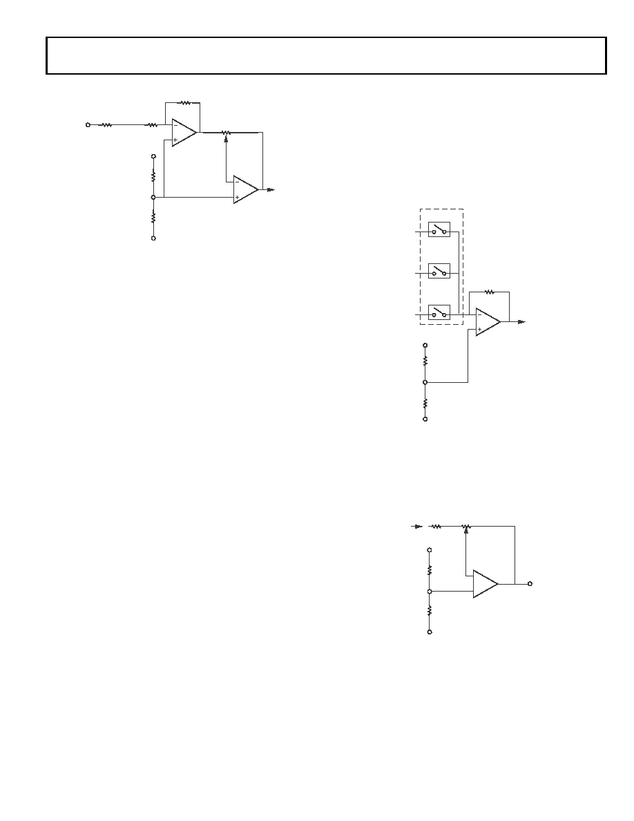
Figure 3. Microphone Input to ADC
ADC
OR
SIDETONE
INTERNAL CIRCUITRY
MICIN
AVDD
VMID
AGND
REXT
10kΩ
50kΩ
0dB/20dB/40dB
GAIN BOOST
Figure 4. Output Signal Chain
Figure 5. Headphone Output
LINE OUTPUT
AND
HEADPHONE
OUTPUT
AVDD
VMID
AGND
BYPASS
SIDETONE
DACSEL
LINE
INPUT
MICROPHONE
INPUT
DAC
OUTPUT
INTERNAL CIRCUITRY
RHPOUT
or
LHPOUT
DAC/
SIDETONE/
BYPASS
AVDD
VMID
AGND
+
–
INTERNAL CIRCUITRY
相关PDF资料 |
PDF描述 |
|---|---|
| REC3-1215DR/H1M/SMD | CONV DC/DC 3W 12VIN +/-15VOUT |
| VE-J5B-IZ | CONVERTER MOD DC/DC 95V 25W |
| MAX6519UKP045+T | IC TEMP SENSOR SW SOT23-5 |
| VI-23Y-CX-F2 | CONVERTER MOD DC/DC 3.3V 49.5W |
| VI-23Y-CW-F4 | CONVERTER MOD DC/DC 3.3V 66W |
相关代理商/技术参数 |
参数描述 |
|---|---|
| ADSP-BF523BBCZ-5A | 功能描述:IC DSP 16BIT 533MHZ 208CSPBGA RoHS:是 类别:集成电路 (IC) >> 嵌入式 - DSP(数字式信号处理器) 系列:Blackfin® 标准包装:40 系列:TMS320DM64x, DaVinci™ 类型:定点 接口:I²C,McASP,McBSP 时钟速率:400MHz 非易失内存:外部 芯片上RAM:160kB 电压 - 输入/输出:3.30V 电压 - 核心:1.20V 工作温度:0°C ~ 90°C 安装类型:表面贴装 封装/外壳:548-BBGA,FCBGA 供应商设备封装:548-FCBGA(27x27) 包装:托盘 配用:TMDSDMK642-0E-ND - DEVELPER KIT W/NTSC CAMERA296-23038-ND - DSP STARTER KIT FOR TMS320C6416296-23059-ND - FLASHBURN PORTING KIT296-23058-ND - EVAL MODULE FOR DM642TMDSDMK642-ND - DEVELOPER KIT W/NTSC CAMERA |
| ADSP-BF523KBCZ-5 | 功能描述:IC DSP 16BIT 533MHZ 289-CSPBGA RoHS:是 类别:集成电路 (IC) >> 嵌入式 - DSP(数字式信号处理器) 系列:Blackfin® 标准包装:2 系列:StarCore 类型:SC140 内核 接口:DSI,以太网,RS-232 时钟速率:400MHz 非易失内存:外部 芯片上RAM:1.436MB 电压 - 输入/输出:3.30V 电压 - 核心:1.20V 工作温度:-40°C ~ 105°C 安装类型:表面贴装 封装/外壳:431-BFBGA,FCBGA 供应商设备封装:431-FCPBGA(20x20) 包装:托盘 |
| ADSP-BF523KBCZ-5C2 | 功能描述:IC DSP 16BIT 533MHZ 289CSPBGA RoHS:是 类别:集成电路 (IC) >> 嵌入式 - DSP(数字式信号处理器) 系列:Blackfin® 标准包装:40 系列:TMS320DM64x, DaVinci™ 类型:定点 接口:I²C,McASP,McBSP 时钟速率:400MHz 非易失内存:外部 芯片上RAM:160kB 电压 - 输入/输出:3.30V 电压 - 核心:1.20V 工作温度:0°C ~ 90°C 安装类型:表面贴装 封装/外壳:548-BBGA,FCBGA 供应商设备封装:548-FCBGA(27x27) 包装:托盘 配用:TMDSDMK642-0E-ND - DEVELPER KIT W/NTSC CAMERA296-23038-ND - DSP STARTER KIT FOR TMS320C6416296-23059-ND - FLASHBURN PORTING KIT296-23058-ND - EVAL MODULE FOR DM642TMDSDMK642-ND - DEVELOPER KIT W/NTSC CAMERA |
| ADSP-BF523KBCZ-6 | 功能描述:IC DSP 16BIT 600MHZ 289-CSPBGA RoHS:是 类别:集成电路 (IC) >> 嵌入式 - DSP(数字式信号处理器) 系列:Blackfin® 标准包装:2 系列:StarCore 类型:SC140 内核 接口:DSI,以太网,RS-232 时钟速率:400MHz 非易失内存:外部 芯片上RAM:1.436MB 电压 - 输入/输出:3.30V 电压 - 核心:1.20V 工作温度:-40°C ~ 105°C 安装类型:表面贴装 封装/外壳:431-BFBGA,FCBGA 供应商设备封装:431-FCPBGA(20x20) 包装:托盘 |
| ADSP-BF523KBCZ-6A | 功能描述:IC DSP CTRLR 16B 600MHZ 208BGA RoHS:是 类别:集成电路 (IC) >> 嵌入式 - DSP(数字式信号处理器) 系列:Blackfin® 标准包装:2 系列:StarCore 类型:SC140 内核 接口:DSI,以太网,RS-232 时钟速率:400MHz 非易失内存:外部 芯片上RAM:1.436MB 电压 - 输入/输出:3.30V 电压 - 核心:1.20V 工作温度:-40°C ~ 105°C 安装类型:表面贴装 封装/外壳:431-BFBGA,FCBGA 供应商设备封装:431-FCPBGA(20x20) 包装:托盘 |
发布紧急采购,3分钟左右您将得到回复。