- 您现在的位置:买卖IC网 > PDF目录19397 > ADSP-BF526KBCZ-3 (Analog Devices Inc)IC DSP CTRLR 300MHZ 289CSPBGA PDF资料下载
参数资料
| 型号: | ADSP-BF526KBCZ-3 |
| 厂商: | Analog Devices Inc |
| 文件页数: | 31/88页 |
| 文件大小: | 0K |
| 描述: | IC DSP CTRLR 300MHZ 289CSPBGA |
| 标准包装: | 1 |
| 系列: | Blackfin® |
| 类型: | 定点 |
| 接口: | DMA,以太网,I²C,PPI,SPI,SPORT,UART,USB |
| 时钟速率: | 300MHz |
| 非易失内存: | ROM(32 kB) |
| 芯片上RAM: | 132kB |
| 电压 - 输入/输出: | 1.8V,2.5V,3.3V |
| 电压 - 核心: | 1.30V |
| 工作温度: | 0°C ~ 70°C |
| 安装类型: | 表面贴装 |
| 封装/外壳: | 289-LFBGA,CSPBGA |
| 供应商设备封装: | 289-CSPBGA(12x12) |
| 包装: | 托盘 |
第1页第2页第3页第4页第5页第6页第7页第8页第9页第10页第11页第12页第13页第14页第15页第16页第17页第18页第19页第20页第21页第22页第23页第24页第25页第26页第27页第28页第29页第30页当前第31页第32页第33页第34页第35页第36页第37页第38页第39页第40页第41页第42页第43页第44页第45页第46页第47页第48页第49页第50页第51页第52页第53页第54页第55页第56页第57页第58页第59页第60页第61页第62页第63页第64页第65页第66页第67页第68页第69页第70页第71页第72页第73页第74页第75页第76页第77页第78页第79页第80页第81页第82页第83页第84页第85页第86页第87页第88页
�� �
�
�ADSP-BF522/ADSP-BF523/ADSP-BF524/ADSP-BF525/ADSP-BF526/ADSP-BF527�
�Clock� Related� Operating� Conditions�
�for� ADSP-BF523/ADSP-BF525/ADSP-BF527� Processors�
��ADSP-BF523/ADSP-BF525/ADSP-BF527� processors.� Take� care�
�Use� the� nominal� voltage� setting� (� Table� 15� )� for� internal� and�
�external� regulators.�
�in� selecting� MSEL,� SSEL,� and� CSEL� ratios� so� as� not� to� exceed� the�
��describes� phase-locked� loop� operating� conditions.�
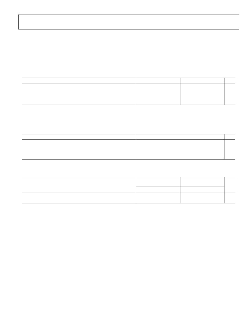
�Table� 15.� Core� Clock� (CCLK)� Requirements� (All� Instruction� Rates� 1� )� for� ADSP-BF523/ADSP-BF525/ADSP-BF527� Processors�
�Parameter�
�Nominal� Voltage� Setting�
�Max�
�Unit�
�f� CCLK�
�f� CCLK�
�f� CCLK�
�f� CCLK�
�Core� Clock� Frequency� (V� DDINT� =1.14� V� minimum)�
�Core� Clock� Frequency� (V� DDINT� =1.093� V� minimum)�
�Core� Clock� Frequency� (V� DDINT� =� 1.045� V� minimum)� 4�
�Core� Clock� Frequency� (V� DDINT� =� 0.95� V� minimum)�
�1.20� V�
�1.15� V�
�1.10� V�
�1.0� V�
�600� 2�
�533� 3�
�400�
�400�
�MHz�
�MHz�
�MHz�
�MHz�
�1�
�2�
�3�
�4�
�����Table� 16.� Phase-Locked� Loop� Operating� Conditions� for� ADSP-BF523/ADSP-BF525/ADSP-BF527� Processors�
�Parameter�
�Min�
�Max�
�Unit�
�f� VCO�
�Voltage� Controlled� Oscillator� (VCO)� Frequency�
�60�
�Instruction� Rate� 1�
�MHz�
�(Commercial/Industrial� Models)�
�f� VCO�
�Voltage� Controlled� Oscillator� (VCO)� Frequency�
�70�
�Instruction� Rate� 1�
�MHz�
�(Automotive� Models)�
�1�
��Table� 17.� SCLK� Conditions� for� ADSP-BF523/ADSP-BF525/ADSP-BF527� Processors�
�V� DDEXT� /V� DDMEM�
�1.8� V� Nominal� 1�
�V� DDEXT� /V� DDMEM�
�2.5� V� or� 3.3� V� Nominal�
�Parameter�
�Max�
�Max�
�Unit�
�f� SCLK�
�CLKOUT/SCLK� Frequency� (V� DDINT� ≥� 1.14� V)�
�2�
�100�
�133� 3�
�MHz�
�f� SCLK�
�CLKOUT/SCLK� Frequency� (V� DDINT� <� 1.14� V)� 2�
�100�
�100�
�MHz�
�1�
�2�
�3�
�If� either� V� DDEXT� or� V� DDMEM� are� operating� at� 1.8� V� nominal,� f� SCLK� is� constrained� to� 100� MHz.�
�f� SCLK� must� be� less� than� or� equal� to� f� CCLK� and� is� subject� to� additional� restrictions� for� SDRAM� interface� operation.� See� Table� 38� on� Page� 47� .�
�Rounded� number.� Actual� test� specification� is� SCLK� period� of� 7.5� ns.� See� Table� 38� on� Page� 47� .�
�Rev.� D� |�
�Page� 31� of� 88� |� July� 2013�
�相关PDF资料 |
PDF描述 |
|---|---|
| TRJC107K010RRJ | CAP TANT 100UF 10V 10% 2312 |
| ECM12DRKI | CONN EDGECARD 24POS DIP .156 SLD |
| ECM08DRAI | CONN EDGECARD 16POS R/A .156 SLD |
| TAP156K025BRS | CAP TANT 15UF 25V 10% RADIAL |
| ADSP-21478KSWZ-2A | IC DSP SHARC 266MHZ LP 100LQFP |
相关代理商/技术参数 |
参数描述 |
|---|---|
| ADSP-BF526KBCZ-3C2 | 功能描述:IC DSP CTRLR 300MHZ 289CSPBGA RoHS:是 类别:集成电路 (IC) >> 嵌入式 - DSP(数字式信号处理器) 系列:Blackfin® 标准包装:2 系列:StarCore 类型:SC140 内核 接口:DSI,以太网,RS-232 时钟速率:400MHz 非易失内存:外部 芯片上RAM:1.436MB 电压 - 输入/输出:3.30V 电压 - 核心:1.20V 工作温度:-40°C ~ 105°C 安装类型:表面贴装 封装/外壳:431-BFBGA,FCBGA 供应商设备封装:431-FCPBGA(20x20) 包装:托盘 |
| ADSP-BF526KBCZ-4 | 功能描述:IC DSP CTRLR 400MHZ 289CSPBGA RoHS:是 类别:集成电路 (IC) >> 嵌入式 - DSP(数字式信号处理器) 系列:Blackfin® 标准包装:2 系列:StarCore 类型:SC140 内核 接口:DSI,以太网,RS-232 时钟速率:400MHz 非易失内存:外部 芯片上RAM:1.436MB 电压 - 输入/输出:3.30V 电压 - 核心:1.20V 工作温度:-40°C ~ 105°C 安装类型:表面贴装 封装/外壳:431-BFBGA,FCBGA 供应商设备封装:431-FCPBGA(20x20) 包装:托盘 |
| ADSP-BF526KBCZ-4C2 | 功能描述:IC DSP CTRLR 400MHZ 289CSPBGA RoHS:是 类别:集成电路 (IC) >> 嵌入式 - DSP(数字式信号处理器) 系列:Blackfin® 标准包装:2 系列:StarCore 类型:SC140 内核 接口:DSI,以太网,RS-232 时钟速率:400MHz 非易失内存:外部 芯片上RAM:1.436MB 电压 - 输入/输出:3.30V 电压 - 核心:1.20V 工作温度:-40°C ~ 105°C 安装类型:表面贴装 封装/外壳:431-BFBGA,FCBGA 供应商设备封装:431-FCPBGA(20x20) 包装:托盘 |
| ADSP-BF526KBCZ4C2X | 制造商:Analog Devices 功能描述:DSP 32-BIT 400MHZ - Trays |
| ADSP-BF526KBCZ-4X | 制造商:Analog Devices 功能描述:LOW POWER BLACKFIN PROCESSOR WITH ADVANCED PERIPHERALS AND L - Trays |
发布紧急采购,3分钟左右您将得到回复。