- 您现在的位置:买卖IC网 > PDF目录11722 > ADUC7022BCPZ32 (Analog Devices Inc)IC MCU FLSH 32K ANLG I/O 40LFCSP PDF资料下载
参数资料
| 型号: | ADUC7022BCPZ32 |
| 厂商: | Analog Devices Inc |
| 文件页数: | 84/104页 |
| 文件大小: | 0K |
| 描述: | IC MCU FLSH 32K ANLG I/O 40LFCSP |
| 产品培训模块: | ARM7 Applications & Tools Intro to ARM7 Core & Microconverters |
| 标准包装: | 1 |
| 系列: | MicroConverter® ADuC7xxx |
| 核心处理器: | ARM7 |
| 芯体尺寸: | 16/32-位 |
| 速度: | 44MHz |
| 连通性: | EBI/EMI,I²C,SPI,UART/USART |
| 外围设备: | PLA,PWM,PSM,温度传感器,WDT |
| 输入/输出数: | 13 |
| 程序存储器容量: | 32KB(16K x 16) |
| 程序存储器类型: | 闪存 |
| RAM 容量: | 1K x 32 |
| 电压 - 电源 (Vcc/Vdd): | 2.7 V ~ 3.6 V |
| 数据转换器: | A/D 10x12b |
| 振荡器型: | 内部 |
| 工作温度: | -40°C ~ 125°C |
| 封装/外壳: | 40-VFQFN 裸露焊盘,CSP |
| 包装: | 托盘 |
第1页第2页第3页第4页第5页第6页第7页第8页第9页第10页第11页第12页第13页第14页第15页第16页第17页第18页第19页第20页第21页第22页第23页第24页第25页第26页第27页第28页第29页第30页第31页第32页第33页第34页第35页第36页第37页第38页第39页第40页第41页第42页第43页第44页第45页第46页第47页第48页第49页第50页第51页第52页第53页第54页第55页第56页第57页第58页第59页第60页第61页第62页第63页第64页第65页第66页第67页第68页第69页第70页第71页第72页第73页第74页第75页第76页第77页第78页第79页第80页第81页第82页第83页当前第84页第85页第86页第87页第88页第89页第90页第91页第92页第93页第94页第95页第96页第97页第98页第99页第100页第101页第102页第103页第104页
ADuC7019/20/21/22/24/25/26/27/28/29
Data Sheet
Rev. F | Page 80 of 104
PROGRAMMABLE LOGIC ARRAY (PLA)
Every ADuC7019/20/21/22/24/25/26/27/28/29 integrates a
fully programmable logic array (PLA) that consists of two
independent but interconnected PLA blocks. Each block
consists of eight PLA elements, giving each part a total of
16 PLA elements.
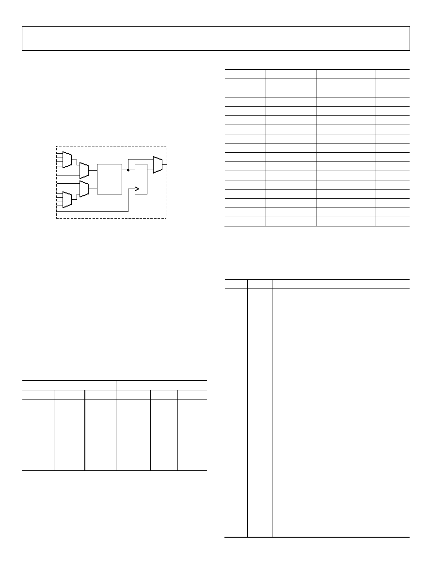
Each PLA element contains a two-input lookup table that can
be configured to generate any logic output function based on
two inputs and a flip-flop. This is represented in Figure 76.
04
95
5-
0
33
4
2
0
1
3
A
B
LOOKUP
TABLE
Figure 76. PLA Element
In total, 30 GPIO pins are available on each ADuC7019/20/21/
22/24/25/26/27/28/29 for the PLA. These include 16 input pins
and 14 output pins, which msut be configured in the GPxCON
register as PLA pins before using the PLA. Note that the
comparator output is also included as one of the 16 input pins.
The PLA is configured via a set of user MMRs. The output(s) of
the PLA can be routed to the internal interrupt system, to the
CONVSTART signal of the ADC, to an MMR, or to any of the 16
PLA output pins.
The two blocks can be interconnected as follows:
Output of Element 15 (Block 1) can be fed back to Input 0
of Mux 0 of Element 0 (Block 0).
Output of Element 7 (Block 0) can be fed back to the Input 0
of Mux 0 of Element 8 (Block 1).
Table 145. Element Input/Output
PLA Block 0
PLA Block 1
Element
Input
Output
Element
Input
Output
0
P1.0
P1.7
8
P3.0
P4.0
1
P1.1
P0.4
9
P3.1
P4.1
2
P1.2
P0.5
10
P3.2
P4.2
3
P1.3
P0.6
11
P3.3
P4.3
4
P1.4
P0.7
12
P3.4
P4.4
5
P1.5
P2.0
13
P3.5
P4.5
6
P1.6
P2.1
14
P3.6
P4.6
7
P0.0
P2.2
15
P3.7
P4.7
PLA MMRs Interface
The PLA peripheral interface consists of the 22 MMRs
described in this section.
Table 146. PLAELMx Registers
Name
Address
Default Value
Access
PLAELM0
0xFFFF0B00
0x0000
R/W
PLAELM1
0xFFFF0B04
0x0000
R/W
PLAELM2
0xFFFF0B08
0x0000
R/W
PLAELM3
0xFFFF0B0C
0x0000
R/W
PLAELM4
0xFFFF0B10
0x0000
R/W
PLAELM5
0xFFFF0B14
0x0000
R/W
PLAELM6
0xFFFF0B18
0x0000
R/W
PLAELM7
0xFFFF0B1C
0x0000
R/W
PLAELM8
0xFFFF0B20
0x0000
R/W
PLAELM9
0xFFFF0B24
0x0000
R/W
PLAELM10
0xFFFF0B28
0x0000
R/W
PLAELM11
0xFFFF0B2C
0x0000
R/W
PLAELM12
0xFFFF0B30
0x0000
R/W
PLAELM13
0xFFFF0B34
0x0000
R/W
PLAELM14
0xFFFF0B38
0x0000
R/W
PLAELM15
0xFFFF0B3C
0x0000
R/W
PLAELMx are Element 0 to Element 15 control registers. They
configure the input and output mux of each element, select the
function in the lookup table, and bypass/use the flip-flop. See
Table 147. PLAELMx MMR Bit Descriptions
Bit
Value
Description
31:11
Reserved.
10:9
Mux 0 control (see Table 152).
8:7
Mux 1 control (see Table 152).
6
Mux 2 control. Set by user to select the output
of Mux 0. Cleared by user to select the bit value
from PLADIN.
5
Mux 3 control. Set by user to select the input
pin of the particular element. Cleared by user to
select the output of Mux 1.
4:1
Lookup table control.
0000
0.
0001
NOR.
0010
B AND NOT A.
0011
NOT A.
0100
A AND NOT B.
0101
NOT B.
0110
EXOR.
0111
NAND.
1000
AND.
1001
EXNOR.
1010
B.
1011
NOT A OR B.
1100
A.
1101
A OR NOT B.
1110
OR.
1111
1.
0
Mux 4 control. Set by user to bypass the flip-
flop. Cleared by user to select the flip-flop
(cleared by default).
相关PDF资料 |
PDF描述 |
|---|---|
| VE-BTJ-IX-F1 | CONVERTER MOD DC/DC 36V 75W |
| ADUC7023BCPZ62I | IC MCU 12BIT 62KB FLASH 32LFCSP |
| D38999/26MB98HN | CONN PLUG 6POS STRAIGHT W/PINS |
| VE-B7L-IW-F1 | CONVERTER MOD DC/DC 28V 100W |
| AT89LP51-20PU | MCU 8051 4K FLASH 20MHZ |
相关代理商/技术参数 |
参数描述 |
|---|---|
| ADUC7022BCPZ32-RL | 功能描述:IC MCU 12BIT 1MSPS UART 40-LFCSP RoHS:是 类别:集成电路 (IC) >> 嵌入式 - 微控制器, 系列:MicroConverter® ADuC7xxx 标准包装:38 系列:Encore!® XP® 核心处理器:eZ8 芯体尺寸:8-位 速度:5MHz 连通性:IrDA,UART/USART 外围设备:欠压检测/复位,LED,POR,PWM,WDT 输入/输出数:16 程序存储器容量:4KB(4K x 8) 程序存储器类型:闪存 EEPROM 大小:- RAM 容量:1K x 8 电压 - 电源 (Vcc/Vdd):2.7 V ~ 3.6 V 数据转换器:- 振荡器型:内部 工作温度:-40°C ~ 105°C 封装/外壳:20-SOIC(0.295",7.50mm 宽) 包装:管件 其它名称:269-4116Z8F0413SH005EG-ND |
| ADUC7022BCPZ32-RL7 | 制造商:Analog Devices 功能描述:MCU 16-bit/32-bit ADuC7xxx ARM7TDMI RISC 32KB Flash 3.3V 40-Pin LFCSP EP T/R |
| ADUC7022BCPZ62 | 功能描述:IC MCU FLSH 62K ANLG I/O 40LFCSP RoHS:是 类别:集成电路 (IC) >> 嵌入式 - 微控制器, 系列:MicroConverter® ADuC7xxx 标准包装:250 系列:LPC11Uxx 核心处理器:ARM? Cortex?-M0 芯体尺寸:32-位 速度:50MHz 连通性:I²C,Microwire,SPI,SSI,SSP,UART/USART,USB 外围设备:欠压检测/复位,POR,WDT 输入/输出数:40 程序存储器容量:96KB(96K x 8) 程序存储器类型:闪存 EEPROM 大小:4K x 8 RAM 容量:10K x 8 电压 - 电源 (Vcc/Vdd):1.8 V ~ 3.6 V 数据转换器:A/D 8x10b 振荡器型:内部 工作温度:-40°C ~ 85°C 封装/外壳:48-LQFP 包装:托盘 其它名称:568-9587 |
| ADUC7022BCPZ62-RL | 制造商:Analog Devices 功能描述:MCU 16-Bit/32-Bit ADuC7xxx ARM7TDMI RISC 62KB Flash 3.3V 40-Pin LFCSP EP T/R |
| ADUC7022BCPZ62-RL7 | 功能描述:IC MSU 12BIT 1MSPS UART 40-LFCSP RoHS:是 类别:集成电路 (IC) >> 嵌入式 - 微控制器, 系列:MicroConverter® ADuC7xxx 标准包装:38 系列:Encore!® XP® 核心处理器:eZ8 芯体尺寸:8-位 速度:5MHz 连通性:IrDA,UART/USART 外围设备:欠压检测/复位,LED,POR,PWM,WDT 输入/输出数:16 程序存储器容量:4KB(4K x 8) 程序存储器类型:闪存 EEPROM 大小:- RAM 容量:1K x 8 电压 - 电源 (Vcc/Vdd):2.7 V ~ 3.6 V 数据转换器:- 振荡器型:内部 工作温度:-40°C ~ 105°C 封装/外壳:20-SOIC(0.295",7.50mm 宽) 包装:管件 其它名称:269-4116Z8F0413SH005EG-ND |
发布紧急采购,3分钟左右您将得到回复。