- 您现在的位置:买卖IC网 > PDF目录11205 > ADUC7025BSTZ62-RL (Analog Devices Inc)IC MCU 12BIT 1MSPS UART 64-LQFP PDF资料下载
参数资料
| 型号: | ADUC7025BSTZ62-RL |
| 厂商: | Analog Devices Inc |
| 文件页数: | 98/104页 |
| 文件大小: | 0K |
| 描述: | IC MCU 12BIT 1MSPS UART 64-LQFP |
| 标准包装: | 1,500 |
| 系列: | MicroConverter® ADuC7xxx |
| 核心处理器: | ARM7 |
| 芯体尺寸: | 16/32-位 |
| 速度: | 44MHz |
| 连通性: | EBI/EMI,I²C,SPI,UART/USART |
| 外围设备: | PLA,PWM,PSM,温度传感器,WDT |
| 输入/输出数: | 30 |
| 程序存储器容量: | 64KB(32K x 16) |
| 程序存储器类型: | 闪存 |
| RAM 容量: | 2K x 32 |
| 电压 - 电源 (Vcc/Vdd): | 2.7 V ~ 3.6 V |
| 数据转换器: | A/D 12x12b |
| 振荡器型: | 内部 |
| 工作温度: | -40°C ~ 125°C |
| 封装/外壳: | 64-LQFP |
| 包装: | 带卷 (TR) |
第1页第2页第3页第4页第5页第6页第7页第8页第9页第10页第11页第12页第13页第14页第15页第16页第17页第18页第19页第20页第21页第22页第23页第24页第25页第26页第27页第28页第29页第30页第31页第32页第33页第34页第35页第36页第37页第38页第39页第40页第41页第42页第43页第44页第45页第46页第47页第48页第49页第50页第51页第52页第53页第54页第55页第56页第57页第58页第59页第60页第61页第62页第63页第64页第65页第66页第67页第68页第69页第70页第71页第72页第73页第74页第75页第76页第77页第78页第79页第80页第81页第82页第83页第84页第85页第86页第87页第88页第89页第90页第91页第92页第93页第94页第95页第96页第97页当前第98页第99页第100页第101页第102页第103页第104页
Data Sheet
ADuC7019/20/21/22/24/25/26/27/28/29
Rev. F | Page 93 of 104
HARDWARE DESIGN CONSIDERATIONS
POWER SUPPLIES
The ADuC7019/20/21/22/24/25/26/27/28/29 operational power
supply voltage range is 2.7 V to 3.6 V. Separate analog and
digital power supply pins (AVDD and IOVDD, respectively) allow
AVDD to be kept relatively free of noisy digital signals often
present on the system IOVDD line. In this mode, the part can
also operate with split supplies; that is, it can use different
voltage levels for each supply. For example, the system can
be designed to operate with an IOVDD voltage level of 3.3 V
whereas the AVDD level can be at 3 V or vice versa. A typical
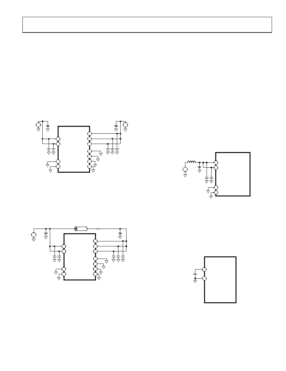
split supply configuration is shown in Figure 87.
04955-
044
ADuC7026
0.1F
ANALOG
SUPPLY
10F
73
74
AVDD
75
DACVDD
8
GNDREF
70
DACGND
71
AGND
67
REFGND
26
IOVDD
54
25
IOGND
53
0.1F
+
–
DIGITAL
SUPPLY
10F
+
–
Figure 87. External Dual Supply Connections
As an alternative to providing two separate power supplies, the
user can reduce noise on AVDD by placing a small series resistor
and/or ferrite bead between AVDD and IOVDD and then decoupling
AVDD separately to ground. An example of this configuration is
shown in Figure 88. With this configuration, other analog circuitry
(such as op amps and voltage reference) can be powered from
the AVDD supply line as well.
04955-
045
ADuC7026
0.1F
BEAD
1.6
73
74
AVDD
75
DACVDD
8
GNDREF
70
DACGND
71
AGND
67
REFGND
26
IOVDD
54
25
IOGND
53
0.1F
DIGITAL SUPPLY
10F
+
–
Figure 88. External Single Supply Connections
Note that in both Figure 87 and Figure 88, a large value (10 F)
reservoir capacitor sits on IOVDD, and a separate 10 F capacitor
sits on AVDD. In addition, local small-value (0.1 F) capacitors are
located at each AVDD and IOVDD pin of the chip. As per standard
design practice, be sure to include all of these capacitors and ensure
that the smaller capacitors are close to each AVDD pin with trace
lengths as short as possible. Connect the ground terminal of
each of these capacitors directly to the underlying ground plane.
Finally, note that the analog and digital ground pins on the
ADuC7019/20/21/22/24/25/26/27/28/29 must be referenced to
the same system ground reference point at all times.
IOVDD Supply Sensitivity
The IOVDD supply is sensitive to high frequency noise because it
is the supply source for the internal oscillator and PLL circuits.
When the internal PLL loses lock, the clock source is removed
by a gating circuit from the CPU, and the ARM7TDMI core
stops executing code until the PLL regains lock. This feature
ensures that no flash interface timings or ARM7TDMI timings
are violated.
Typically, frequency noise greater than 50 kHz and 50 mV p-p
on top of the supply causes the core to stop working.
If decoupling values recommended in the Power Supplies
section do not sufficiently dampen all noise sources below
is recommended.
ADuC7026
26
IOVDD
54
25
IOGND
53
0.1F
DIGITAL
SUPPLY
10F
+
–
1H
04955-
087
Figure 89. Recommended IOVDD Supply Filter
Linear Voltage Regulator
Each ADuC7019/20/21/22/24/25/26/27/28/29 requires a single
3.3 V supply, but the core logic requires a 2.6 V supply. An on-
chip linear regulator generates the 2.6 V from IOVDD for the
core logic. The LVDD pin is the 2.6 V supply for the core logic.
An external compensation capacitor of 0.47 F must be
connected between LVDD and DGND (as close as possible to
these pins) to act as a tank of charge as shown in Figure 90.
04955-
046
ADuC7026
0.47
mF
27 LVDD
28 DGND
Figure 90. Voltage Regulator Connections
The LVDD pin should not be used for any other chip. It is also
recommended to use excellent power supply decoupling on
IOVDD to help improve line regulation performance of the on-
chip voltage regulator.
相关PDF资料 |
PDF描述 |
|---|---|
| ADUC7025BCPZ62-RL | IC MCU 12BIT 1MSPS UART 64-LFCSP |
| AT91SAM7S256C-AU-999 | IC MCU ARM7 256KB FLASH 64LQFP |
| AT91SAM7X128B-CU-999 | IC MCU ARM 128KB FLASH 100TFBGA |
| VI-J3X-IW-F2 | CONVERTER MOD DC/DC 5.2V 100W |
| VI-J3X-IW-F1 | CONVERTER MOD DC/DC 5.2V 100W |
相关代理商/技术参数 |
参数描述 |
|---|---|
| ADUC7026 | 制造商:AD 制造商全称:Analog Devices 功能描述:Precision Analog Microcontroller 12-bit Analog I/O, ARM7TDMI MCU |
| ADUC7026BST62 | 制造商:AD 制造商全称:Analog Devices 功能描述:Precision Analog Microcontroller 12-bit Analog I/O, ARM7TDMI MCU |
| ADUC7026BST62-U1 | 制造商:Analog Devices 功能描述: |
| ADUC7026BSTZ62 | 功能描述:IC MCU FLASH 62K W/ANLG 80LQFP RoHS:是 类别:集成电路 (IC) >> 嵌入式 - 微控制器, 系列:MicroConverter® ADuC7xxx 标准包装:250 系列:56F8xxx 核心处理器:56800E 芯体尺寸:16-位 速度:60MHz 连通性:CAN,SCI,SPI 外围设备:POR,PWM,温度传感器,WDT 输入/输出数:21 程序存储器容量:40KB(20K x 16) 程序存储器类型:闪存 EEPROM 大小:- RAM 容量:6K x 16 电压 - 电源 (Vcc/Vdd):2.25 V ~ 3.6 V 数据转换器:A/D 6x12b 振荡器型:内部 工作温度:-40°C ~ 125°C 封装/外壳:48-LQFP 包装:托盘 配用:MC56F8323EVME-ND - BOARD EVALUATION MC56F8323 |
| ADUC7026BSTZ62I | 功能描述:IC MCU FLASH 62K ANLG I/0 80LQFP RoHS:是 类别:集成电路 (IC) >> 嵌入式 - 微控制器, 系列:MicroConverter® ADuC7xxx 标准包装:250 系列:LPC11Uxx 核心处理器:ARM? Cortex?-M0 芯体尺寸:32-位 速度:50MHz 连通性:I²C,Microwire,SPI,SSI,SSP,UART/USART,USB 外围设备:欠压检测/复位,POR,WDT 输入/输出数:40 程序存储器容量:96KB(96K x 8) 程序存储器类型:闪存 EEPROM 大小:4K x 8 RAM 容量:10K x 8 电压 - 电源 (Vcc/Vdd):1.8 V ~ 3.6 V 数据转换器:A/D 8x10b 振荡器型:内部 工作温度:-40°C ~ 85°C 封装/外壳:48-LQFP 包装:托盘 其它名称:568-9587 |
发布紧急采购,3分钟左右您将得到回复。