参数资料
| 型号: | ADUC7121BBCZ-RL |
| 厂商: | Analog Devices Inc |
| 文件页数: | 26/96页 |
| 文件大小: | 0K |
| 描述: | PRECISION ANALOG MCU I.C |
| 标准包装: | 1 |
| 系列: | MicroConverter® ADuC7xxx |
| 核心处理器: | ARM7 |
| 芯体尺寸: | 16/32-位 |
| 速度: | 41.78MHz |
| 连通性: | I²C,SPI,UART/USART |
| 外围设备: | POR,PWM,WDT |
| 输入/输出数: | 32 |
| 程序存储器容量: | 126KB(63K x 16) |
| 程序存储器类型: | 闪存 |
| RAM 容量: | 8K x 8 |
| 电压 - 电源 (Vcc/Vdd): | 3 V ~ 3.6 V |
| 数据转换器: | A/D 9x12b,D/A 4x12b |
| 振荡器型: | 内部 |
| 工作温度: | -10°C ~ 95°C |
| 封装/外壳: | 108-LFBGA,CSPBGA |
| 包装: | 标准包装 |
| 其它名称: | ADUC7121BBCZ-RLDKR |
第1页第2页第3页第4页第5页第6页第7页第8页第9页第10页第11页第12页第13页第14页第15页第16页第17页第18页第19页第20页第21页第22页第23页第24页第25页当前第26页第27页第28页第29页第30页第31页第32页第33页第34页第35页第36页第37页第38页第39页第40页第41页第42页第43页第44页第45页第46页第47页第48页第49页第50页第51页第52页第53页第54页第55页第56页第57页第58页第59页第60页第61页第62页第63页第64页第65页第66页第67页第68页第69页第70页第71页第72页第73页第74页第75页第76页第77页第78页第79页第80页第81页第82页第83页第84页第85页第86页第87页第88页第89页第90页第91页第92页第93页第94页第95页第96页
ADuC7121
Data Sheet
Rev. B | Page 32 of 96
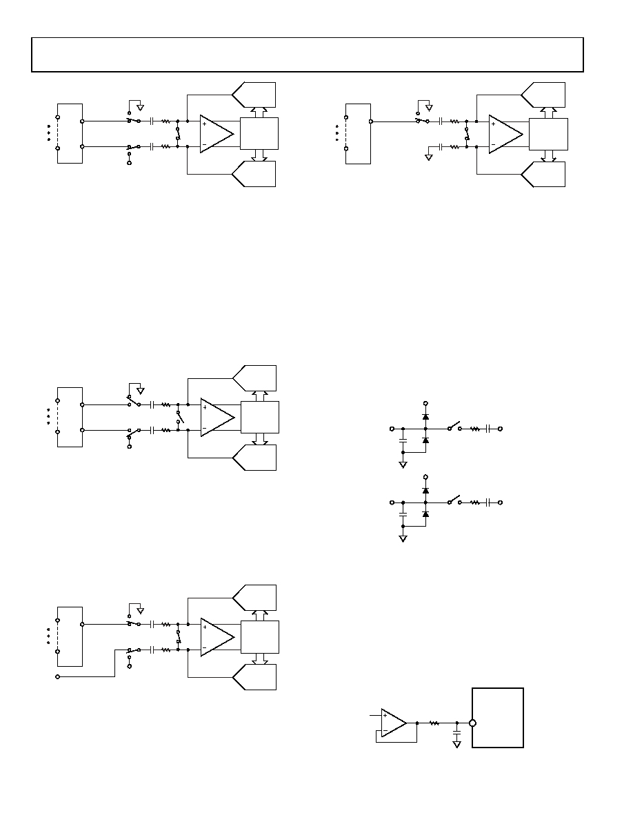
Figure 19. ADC Acquisition Phase
When the ADC starts a conversion (see Figure 20), SW3 opens,
and SW1 and SW2 move to Position B, causing the comparator
to become unbalanced. Both inputs are disconnected as soon as
the conversion begins. The control logic and the charge redistribu-
tion DACs are used to add and subtract fixed amounts of charge
from the sampling capacitor arrays to return the comparator to
a balanced condition. When the comparator is rebalanced, the
conversion is complete.
The control logic generates the ADC output code. The output
impedances of the sources driving the VIN+ input and the VIN
input must be matched; otherwise, the two inputs have different
settling times, resulting in errors.
Figure 20. ADC Conversion Phase
Pseudo Differential Mode
In pseudo differential mode, Channel is linked to the VIN
input of the ADuC7121, and SW2 switches between A
(Channel) and B (VREF). The VIN input must be connected to
ground or a low voltage. The input signal on VIN+ can then vary
from VIN to VREF + VIN. Note that VIN must be chosen so that
VREF + VIN does not exceed AVDD.
Figure 21. ADC in Pseudo Differential Mode
Single-Ended Mode
In single-ended mode, SW2 is always connected internally to
ground. The VIN input pin can be floating. The input signal
range on VIN+ is 0 V to VREF.
Figure 22. ADC in Single-Ended Mode
Analog Input Structure
Figure 23 shows the equivalent circuit of the analog input structure
of the ADC. The four diodes provide ESD protection for the analog
inputs. Take care to ensure that the analog input signals never
exceed the supply rails by more than 300 mV. Voltage in excess
of 300 mV causes these diodes to become forward biased and to
start conducting into the substrate. These diodes can conduct
up to 10 mA without causing irreversible damage to the part.
The C1 capacitors in Figure 23 are typically 4 pF and can be
primarily attributed to pin capacitance. The resistors are lumped
components made up of the on resistance of the switches. The
value of these resistors is typically about 100 Ω. The C2 capacitors
are the ADC sampling capacitors and have a capacitance of
16 pF typical.
Figure 23. Equivalent Analog Input Circuit Conversion Phase: Switches Open,
Track Phase: Switches Closed
For ac applications, removing high frequency components from
the analog input signal is recommended with an RC low-pass
filter on the relevant analog input pins. In applications where
harmonic distortion and signal-to-noise ratio are critical, drive
the analog input from a low impedance source. Large source
impedances significantly affect the ac performance of the ADC
and can necessitate the use of an input buffer amplifier. The choice
of the op amp is a function of the particular application. Figure 24
and Figure 25 give an example of an ADC front end.
Figure 24. Buffering Single-Ended/Pseudo Differential Input
CAPACITIVE
DAC
CAPACITIVE
DAC
CONTROL
LOGIC
COMPARATOR
SW3
SW1
A
B
SW2
CS
VREF
AIN0
AIN11
MUX
CHANNEL+
CHANNEL–
09492-
018
CAPACITIVE
DAC
CAPACITIVE
DAC
CONTROL
LOGIC
COMPARATOR
SW3
SW1
A
B
SW2
CS
VREF
AIN0
AIN11
MUX
CHANNEL+
CHANNEL–
09492
-019
CAPACITIVE
DAC
CAPACITIVE
DAC
CONTROL
LOGIC
COMPARATOR
SW3
SW1
A
B
SW2
CS
VREF
AIN0
AIN11
VIN–
MUX
CHANNEL+
CHANNEL–
09492
-020
CAPACITIVE
DAC
CAPACITIVE
DAC
CONTROL
LOGIC
COMPARATOR
SW3
SW1
A
B
CS
AIN0
AIN11
MUX
CHANNEL+
CHANNEL–
0949
2-
021
AVDD
C1
D
R1 C2
AVDD
C1
D
R1 C2
09
49
2-
0
22
09
49
2-
0
23
ADuC7121
ADC0
10
0.01F
相关PDF资料 |
PDF描述 |
|---|---|
| ADUC7122BBCZ-RL | PRECISION ANALOG MCU I.C |
| ADUC7126BSTZ126-RL | IC MCU 16/32B 126KB FLASH 80LQFP |
| ADUC7129BSTZ126 | IC DAS MCU ARM7 ADC/DDS 80-LQFP |
| ADUC812BSZ-REEL | IC MCU FLASH 12BIT ADC 52MQFP |
| ADUC814BRU | IC ADC 12BIT W/FLASH MCU 28TSSOP |
相关代理商/技术参数 |
参数描述 |
|---|---|
| ADUC7122 | 制造商:AD 制造商全称:Analog Devices 功能描述:Precision Analog Microcontroller, 12-Bit Analog I/O, ARM7TDMI? MCU |
| ADUC7122BBCZ | 功能描述:IC ARM7TDMI MCU 126KB 108CSPBGA RoHS:是 类别:集成电路 (IC) >> 嵌入式 - 微控制器, 系列:MicroConverter® ADuC7xxx 标准包装:250 系列:56F8xxx 核心处理器:56800E 芯体尺寸:16-位 速度:60MHz 连通性:CAN,SCI,SPI 外围设备:POR,PWM,温度传感器,WDT 输入/输出数:21 程序存储器容量:40KB(20K x 16) 程序存储器类型:闪存 EEPROM 大小:- RAM 容量:6K x 16 电压 - 电源 (Vcc/Vdd):2.25 V ~ 3.6 V 数据转换器:A/D 6x12b 振荡器型:内部 工作温度:-40°C ~ 125°C 封装/外壳:48-LQFP 包装:托盘 配用:MC56F8323EVME-ND - BOARD EVALUATION MC56F8323 |
| ADUC7122BBCZ-RL | 功能描述:PRECISION ANALOG MCU I.C RoHS:是 类别:集成电路 (IC) >> 嵌入式 - 微控制器, 系列:MicroConverter® ADuC7xxx 标准包装:38 系列:Encore!® XP® 核心处理器:eZ8 芯体尺寸:8-位 速度:5MHz 连通性:IrDA,UART/USART 外围设备:欠压检测/复位,LED,POR,PWM,WDT 输入/输出数:16 程序存储器容量:4KB(4K x 8) 程序存储器类型:闪存 EEPROM 大小:- RAM 容量:1K x 8 电压 - 电源 (Vcc/Vdd):2.7 V ~ 3.6 V 数据转换器:- 振荡器型:内部 工作温度:-40°C ~ 105°C 封装/外壳:20-SOIC(0.295",7.50mm 宽) 包装:管件 其它名称:269-4116Z8F0413SH005EG-ND |
| ADUC7124 | 制造商:AD 制造商全称:Analog Devices 功能描述:Precision Analog Microcontroller, 12-Bit Analog I/O, Large Memory, ARM7TDMI MCU with Enhanced IRQ Handler |
| ADUC7124BCPZ126 | 功能描述:IC DAS MCU ARM7 ADC/DDS 64LQFP RoHS:是 类别:集成电路 (IC) >> 嵌入式 - 微控制器, 系列:MicroConverter® ADuC7xxx 标准包装:250 系列:LPC11Uxx 核心处理器:ARM? Cortex?-M0 芯体尺寸:32-位 速度:50MHz 连通性:I²C,Microwire,SPI,SSI,SSP,UART/USART,USB 外围设备:欠压检测/复位,POR,WDT 输入/输出数:40 程序存储器容量:96KB(96K x 8) 程序存储器类型:闪存 EEPROM 大小:4K x 8 RAM 容量:10K x 8 电压 - 电源 (Vcc/Vdd):1.8 V ~ 3.6 V 数据转换器:A/D 8x10b 振荡器型:内部 工作温度:-40°C ~ 85°C 封装/外壳:48-LQFP 包装:托盘 其它名称:568-9587 |
发布紧急采购,3分钟左右您将得到回复。