- 您现在的位置:买卖IC网 > PDF目录11203 > ADUC814ARU (Analog Devices Inc)IC ADC 12BIT W/FLASH MCU 28TSSOP PDF资料下载
参数资料
| 型号: | ADUC814ARU |
| 厂商: | Analog Devices Inc |
| 文件页数: | 2/72页 |
| 文件大小: | 0K |
| 描述: | IC ADC 12BIT W/FLASH MCU 28TSSOP |
| 标准包装: | 50 |
| 系列: | MicroConverter® ADuC8xx |
| 核心处理器: | 8052 |
| 芯体尺寸: | 8-位 |
| 速度: | 16.78MHz |
| 连通性: | I²C,SPI,UART/USART |
| 外围设备: | POR,PSM,温度传感器,WDT |
| 输入/输出数: | 17 |
| 程序存储器容量: | 8KB(8K x 8) |
| 程序存储器类型: | 闪存 |
| EEPROM 大小: | 640 x 8 |
| RAM 容量: | 256 x 8 |
| 电压 - 电源 (Vcc/Vdd): | 2.7 V ~ 5.5 V |
| 数据转换器: | A/D 6x12b; D/A 2x12b |
| 振荡器型: | 内部 |
| 工作温度: | -40°C ~ 125°C |
| 封装/外壳: | 28-TSSOP(0.173",4.40mm 宽) |
| 包装: | 管件 |
| 配用: | EVAL-ADUC814QSZ-ND - KIT DEV FOR ADUC814 MICROCONVRTR |
第1页当前第2页第3页第4页第5页第6页第7页第8页第9页第10页第11页第12页第13页第14页第15页第16页第17页第18页第19页第20页第21页第22页第23页第24页第25页第26页第27页第28页第29页第30页第31页第32页第33页第34页第35页第36页第37页第38页第39页第40页第41页第42页第43页第44页第45页第46页第47页第48页第49页第50页第51页第52页第53页第54页第55页第56页第57页第58页第59页第60页第61页第62页第63页第64页第65页第66页第67页第68页第69页第70页第71页第72页
ADuC814
Rev. A | Page 10 of 72
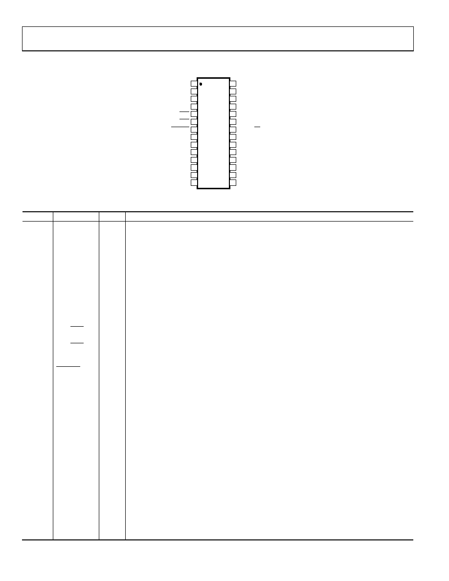
PIN CONFIGURATION AND FUNCTION DESCRIPTION
ADuC814
TOP VIEW
(Not to Scale)
DGND
1
DLOAD
2
P3.0/RxD
3
P3.1/TxD
4
P3.2/INT0
5
DVDD
XTAL2
XTAL1
SCLOCK
P3.7/SDATA/MOSI
28
27
26
25
24
P3.3/INT1
6
P3.4/T0/CONVST
7
P1.0/T2
8
P1.1/T2EX
9
P3.6/MISO
P3.5/T1/SS/EXTCLK
P1.7/ADC5/DAC1
P1.6/ADC4/DAC0
23
22
21
20
RESET 10
P1.5/ADC3
19
P1.2/ADC0 11
P1.3/ADC1 12
AVDD 13
AGND 14
P1.4/ADC2
CREF
VREF
AGND
18
17
16
15
02748-A
-009
Figure 2. Pin Configuration
Table 3. Pin Descriptions
Pin No.
Mnemonic
Type
Function
1
DGND
S
Digital Ground. Ground reference point for the digital circuitry.
2
DLOAD
I
Debug/Serial Download Mode. Enables when pulled high through a resistor on power-on or RESET. In
this mode, DLOAD may also be used as an external emulation I/O pin, therefore the voltage level at
this pin must not be changed during this mode of operation because it may cause an emulation
interrupt that halts code execution. User code is executed when this pin is pulled low on power-on or
RESET.
3–7
P3.0 – P3.4
I/O
Bidirectional Port Pins with Internal Pull-Up Resistors. Port 3 pins that have 1s written to them are
pulled high by the internal pull-up resistors, and in that state they can be used as inputs. As inputs,
with Port 3 pins being pulled low externally, they source current because of the internal pull-up
resistors. When driving a 0-to-1 output transition, a strong pull-up is active during S1 of the
instruction cycle. Port 3 pins also have various secondary functions which are described next.
3
P3.0/RxD
I/O
Receiver Data Input (asynchronous) or Data Input/Output (synchronous) in Serial (UART) Mode.
4
P3.1/TxD
I/O
Transmitter Data Output (asynchronous) or Clock Output (synchronous) in Serial (UART) Mode.
5
P3.2/INT0
I/O
Interrupt 0, programmable edge or level-triggered interrupt input, which can be programmed to one
of two priority levels. This pin can also be used as agate control input to Timer 0.
6
P3.3/INT1
I/O
Interrupt 1, programmable edge or level-triggered interrupt input, which can be programmed to one
of two priority levels. This pin can also be used as agate control input to Timer 1.
7
P3.4/T0/
CONVST
I/O
Timer/Counter 0 Input and External Trigger Input for ADC Conversion Start.
8–9
P1.0–P1.1
I/O
Bidirectional Port Pins with Internal Pull-Up Resistors. Port 1 pins that have 1s written to them are
pulled high by the internal pull-up resistors, and in that state they can be used as inputs. As inputs
,with Port 1 pins being pulled low externally, they source current because of the internal pull-up
resistors When driving a 0-to-1 output transition a strong pull-up is active during S1 of the instruction
cycle. Port 1 pins also have various secondary functions which are described as follows.
8
P1.0/T2
I/O
Timer 2 Digital Input. Input to Timer/Counter 2. When enabled, Counter 2 is incremented in response
to a 1 to 0 transition of the T2 input.
9
P1.1/T2EX
I/O
Digital Input. Capture/Reload trigger for Counter 2.
10
RESET
I
Reset Input. A high level on this pin while the oscillator is running resets the device. There is an
internal weak pull-down and a Schmitt-trigger input stage on this pin.
11–12
P1.2–P1.3
I
Port 1.2 to P1.3. These pins have no digital output drivers, i.e., they can only function as digital inputs,
for which 0 must be written to the port bit. These port pins also have the following analog functionality:
11
P1.2/ADC0
I
ADC Input Channel 0. Selected via ADCCON2 SFR.
12
P1.3/ADC1
I
ADC Input Channel 1. Selected via ADCCON2 SFR.
13
AVDD
S
Analog Positive Supply Voltage, 3 V or 5 V.
14–15
AGND
G
Analog Ground. Ground reference point for the analog circuitry.
16
VREF
I/O
Reference Input/Output. This pin is connected to the internal reference through a switch and is the
reference source for the analog to digital converter. The nominal internal reference voltage is 2.5 V
and this appears at the pin. This pin can be used to connect an external reference to the analog to
digital converter by setting ADCCON1.6 to 1. Connect 0.1 F between this pin and AGND.
相关PDF资料 |
PDF描述 |
|---|---|
| VI-BTK-IX | CONVERTER MOD DC/DC 40V 75W |
| VI-BTK-IW | CONVERTER MOD DC/DC 40V 100W |
| ADUC7128BSTZ126-RL | IC DAS MCU ARM7 ADC/DDS 64-LQFP |
| VI-BTJ-IX | CONVERTER MOD DC/DC 36V 75W |
| VI-BTJ-IW | CONVERTER MOD DC/DC 36V 100W |
相关代理商/技术参数 |
参数描述 |
|---|---|
| ADUC814ARU-D2 | 制造商:Analog Devices 功能描述:12 BIT ADC WITH EMBEDDED 8-BIT MICRO I.C - Tape and Reel 制造商:Rochester Electronics LLC 功能描述:12 BIT ADC WITH EMBEDDED 8-BIT MICRO I.C - Bulk |
| ADUC814ARU-REEL | 制造商:Analog Devices 功能描述:MCU 8-Bit ADuC8xx 8052 CISC 8KB Flash 3V/5V 28-Pin TSSOP T/R 制造商:Analog Devices 功能描述:12 BIT ADC WITH EMBEDDED 8-BIT MICRO I.C - Tape and Reel |
| ADUC814ARU-REEL7 | 制造商:Analog Devices 功能描述:MCU 8-Bit ADuC8xx 8052 CISC 8KB Flash 3V/5V 28-Pin TSSOP T/R 制造商:Analog Devices 功能描述:12 BIT ADC WITH EMBEDDED 8-BIT MICRO I.C - Tape and Reel 制造商:Rochester Electronics LLC 功能描述:12 BIT ADC WITH EMBEDDED 8-BIT MICRO I.C - Tape and Reel |
| ADUC814ARUZ | 功能描述:IC ADC 12BIT W/FLASH MCU 28TSSOP RoHS:是 类别:集成电路 (IC) >> 嵌入式 - 微控制器, 系列:MicroConverter® ADuC8xx 产品培训模块:MCU Product Line Introduction XMEGA Introduction AVR XMEGA USB Connectivity 标准包装:90 系列:AVR® XMEGA 核心处理器:AVR 芯体尺寸:8/16-位 速度:32MHz 连通性:I²C,IrDA,SPI,UART/USART 外围设备:欠压检测/复位,DMA,POR,PWM,WDT 输入/输出数:50 程序存储器容量:192KB(96K x 16) 程序存储器类型:闪存 EEPROM 大小:4K x 8 RAM 容量:16K x 8 电压 - 电源 (Vcc/Vdd):1.6 V ~ 3.6 V 数据转换器:A/D 16x12b; D/A 2x12b 振荡器型:内部 工作温度:-40°C ~ 85°C 封装/外壳:64-TQFP 包装:托盘 配用:ATSTK600-RC14-ND - STK600 SOCKET/ADAPTER 64TQFPATSTK600-TQFP64-ND - STK600 SOCKET/ADAPTER 64-TQFPATAVRONEKIT-ND - KIT AVR/AVR32 DEBUGGER/PROGRMMRATAVRISP2-ND - PROGRAMMER AVR IN SYSTEM |
| ADUC814ARUZ-REEL | 功能描述:IC MCU FLASH 12BIT ADC 28TSSOP RoHS:是 类别:集成电路 (IC) >> 嵌入式 - 微控制器, 系列:MicroConverter® ADuC8xx 标准包装:38 系列:Encore!® XP® 核心处理器:eZ8 芯体尺寸:8-位 速度:5MHz 连通性:IrDA,UART/USART 外围设备:欠压检测/复位,LED,POR,PWM,WDT 输入/输出数:16 程序存储器容量:4KB(4K x 8) 程序存储器类型:闪存 EEPROM 大小:- RAM 容量:1K x 8 电压 - 电源 (Vcc/Vdd):2.7 V ~ 3.6 V 数据转换器:- 振荡器型:内部 工作温度:-40°C ~ 105°C 封装/外壳:20-SOIC(0.295",7.50mm 宽) 包装:管件 其它名称:269-4116Z8F0413SH005EG-ND |
发布紧急采购,3分钟左右您将得到回复。