- 您现在的位置:买卖IC网 > PDF目录21445 > ADUM1401CRWZ-RL (Analog Devices Inc)IC DGITAL ISOLATOR 4CH 16-SOIC PDF资料下载
参数资料
| 型号: | ADUM1401CRWZ-RL |
| 厂商: | Analog Devices Inc |
| 文件页数: | 27/32页 |
| 文件大小: | 0K |
| 描述: | IC DGITAL ISOLATOR 4CH 16-SOIC |
| 设计资源: | 16-Bit Fully Isolated Voltage Output Module Using AD5662, ADuM1401, and External Amplifiers (CN0063) 16-Bit Fully Isolated 4 mA to 20 mA Output Module Using AD5662, ADuM1401, and External Amplifiers (CN0064) 16-Bit Fully Isolated Output Module Using AD5422 and ADuM1401 (CN0065) |
| 其它图纸: | ADUMx4 Series Quad Block Diagram |
| 标准包装: | 1 |
| 系列: | iCoupler® |
| 输入 - 1 侧/2 侧: | 3/1 |
| 通道数: | 4 |
| 电源电压: | 2.7 V ~ 5.5 V |
| 电压 - 隔离: | 2500Vrms |
| 数据速率: | 90Mbps |
| 传输延迟: | 32ns |
| 输出类型: | 逻辑 |
| 封装/外壳: | 16-SOIC(0.295",7.50mm 宽) |
| 供应商设备封装: | 16-SOIC W |
| 包装: | 标准包装 |
| 工作温度: | -40°C ~ 105°C |
| 产品目录页面: | 2766 (CN2011-ZH PDF) |
| 其它名称: | ADUM1401CRWZ-RLDKR |
第1页第2页第3页第4页第5页第6页第7页第8页第9页第10页第11页第12页第13页第14页第15页第16页第17页第18页第19页第20页第21页第22页第23页第24页第25页第26页当前第27页第28页第29页第30页第31页第32页
�� ��
��
��Data� Sheet�
�APPLICATIONS� INFORMATION�
�PC� BOARD� LAYOUT�
�The� ADuM140x� digital� isolator� requires� no� external� interface�
�circuitry� for� the� logic� interfaces.� Power� supply� bypassing� is�
�strongly� recommended� at� the� input� and� output� supply� pins� (see�
�Figure� 17).� Bypass� capacitors� are� most� conveniently� connected�
�between� Pin� 1� and� Pin� 2� for� V� DD1� and� between� Pin� 15� and� Pin� 16�
�for� V� DD2� .� The� capacitor� value� should� be� between� 0.01� μF� and�
�0.1� μF.� The� total� lead� length� between� both� ends� of� the� capacitor�
�and� the� input� power� supply� pin� should� not� exceed� 20� mm.�
�Bypassing� between� Pin� 1� and� Pin� 8� and� between� Pin� 9� and�
�Pin� 16� should� also� be� considered,� unless� the� ground� pair� on�
�each� package� side� is� connected� close� to� the� package.�
�ADuM1400/ADuM1401/ADuM1402�
�DC� CORRECTNESS� AND� MAGNETIC� FIELD�
�IMMUNITY�
�Positive� and� negative� logic� transitions� at� the� isolator� input�
�cause� narrow� (~1� ns)� pulses� to� be� sent� to� the� decoder� via� the�
�transformer.� The� decoder� is� bistable� and� is,� therefore,� either� set�
�or� reset� by� the� pulses,� indicating� input� logic� transitions.� In� the�
�absence� of� logic� transitions� at� the� input� for� more� than� ~1� μs,� a�
�periodic� set� of� refresh� pulses� indicative� of� the� correct� input� state�
�are� sent� to� ensure� dc� correctness� at� the� output.� If� the� decoder�
�receives� no� internal� pulses� of� more� than� about� 5� μs,� the� input�
�side� is� assumed� to� be� unpowered� or� nonfunctional,� in� which�
�case� the� isolator� output� is� forced� to� a� default� state� (see� Table� 15)�
�V� DD1�
�GND� 1�
�V� IA�
�V� IB�
�V� IC� /V� OC�
�V� ID/� V� OD�
�V� DD2�
�GND� 2�
�V� OA�
�V� OB�
�V� OC/� V� IC�
�V� OD/� V� ID�
�by� the� watchdog� timer� circuit.�
�The� limitation� on� the� magnetic� field� immunity� of� the� ADuM140x�
�is� set� by� the� condition� in� which� induced� voltage� in� the� receiving�
�coil� of� the� transformer� is� sufficiently� large� enough� to� either�
�NC/V� E1� V� E2�
�GND� 1� GND� 2�
�Figure� 17.� Recommended� Printed� Circuit� Board� Layout�
�In� applications� involving� high� common-mode� transients,� care�
�should� be� taken� to� ensure� that� board� coupling� across� the� isolation�
�barrier� is� minimized.� Furthermore,� the� board� layout� should� be�
�designed� such� that� any� coupling� that� does� occur� equally� affects�
�all� pins� on� a� given� component� side.� Failure� to� ensure� this� could�
�cause� voltage� differentials� between� pins� exceeding� the� Absolute�
�Maximum� Ratings� of� the� device,� thereby� leading� to� latch-up� or�
�permanent� damage.�
�See� the� AN-1109� Application� Note� for� board� layout� guidelines.�
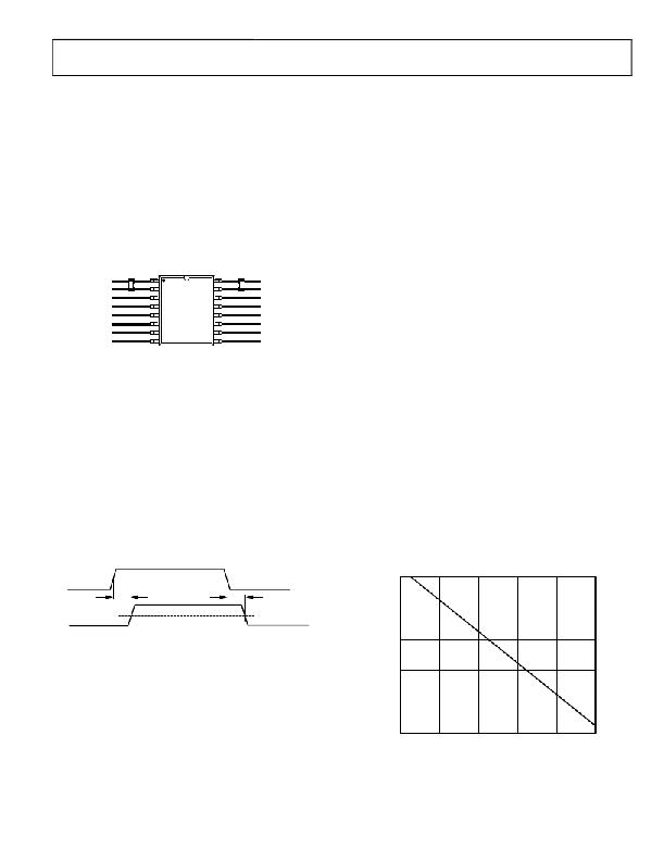
�PROPAGATION� DELAY-RELATED� PARAMETERS�
�Propagation� delay� is� a� parameter� that� describes� the� time� it� takes�
�a� logic� signal� to� propagate� through� a� component.� The� propagation�
�delay� to� a� Logic� 0� output� may� differ� from� the� propagation� delay�
�to� a� Logic� 1� output.�
�falsely� set� or� reset� the� decoder.� The� following� analysis� defines�
�the� conditions� under� which� this� may� occur.� The� 3� V� operating�
�condition� of� the� ADuM140x� is� examined� because� it� represents�
�the� most� susceptible� mode� of� operation.�
�The� pulses� at� the� transformer� output� have� an� amplitude� greater�
�than� 1.0� V.� The� decoder� has� a� sensing� threshold� at� about� 0.5� V,� thus�
�establishing� a� 0.5� V� margin� in� which� induced� voltages� can� be�
�tolerated.� The� voltage� induced� across� the� receiving� coil� is� given� by�
�V� =� (� ?dβ/dt� )� ∑� ∏� r� n2� ;� n� =� 1,� 2,� …� ,� N�
�where:�
�β� is� magnetic� flux� density� (gauss).�
�N� is� the� number� of� turns� in� the� receiving� coil.�
�r� n� is� the� radius� of� the� n� th� turn� in� the� receiving� coil� (cm).�
�Given� the� geometry� of� the� receiving� coil� in� the� ADuM140x� and�
�an� imposed� requirement� that� the� induced� voltage� be� 50%� at�
�most� of� the� 0.5� V� margin� at� the� decoder,� a� maximum� allowable�
�magnetic� field� is� calculated� as� shown� in� Figure� 19.�
�INPUT� (V� Ix� )�
�OUTPUT� (V� Ox� )�
�50%�
�t� PLH�
�t� PHL�
�50%�
�Figure� 18.� Propagation� Delay� Parameters�
�100�
�10�
�1�
�Pulse� width� distortion� is� the� maximum� difference� between�
�these� two� propagation� delay� values� and� is� an� indication� of� how�
�accurately� the� timing� of� the� input� signal� is� preserved.�
�Channel-to-channel� matching� refers� to� the� maximum� amount�
�the� propagation� delay� differs� between� channels� within� a� single�
�ADuM140x� component.�
�0.1�
�0.01�
�Propagation� delay� skew� refers� to� the� maximum� amount� the�
�0.001�
�1k�
�10k�
�100k�
�1M�
�10M�
�100M�
�propagation� delay� differs� between� multiple� ADuM140x�
�components� operating� under� the� same� conditions.�
�Rev.� I� |� Page� 27� of� 32�
�MAGNETIC� FIELD� FREQUENCY� (Hz)�
�Figure� 19.� Maximum� Allowable� External� Magnetic� Flux� Density�
�相关PDF资料 |
PDF描述 |
|---|---|
| 282527-002 | CABLE 1 COND 20AWG SHIELDED |
| 1879455-5 | RES 2.2 OHM 1500W 5% WW LUG |
| PBC-1559-C | COVER ABS FOR PB-1559-BF |
| 152210-0103-GB | CONN 10POS2MM IDCSOCKET GLDW/SR |
| 37108-2165-0W0 FL | CONN PLUG 8POS(4X2) 22-20AWG BLU |
相关代理商/技术参数 |
参数描述 |
|---|---|
| ADUM1401WRWZ | 制造商:Analog Devices 功能描述: |
| ADUM1401WRWZ-RL | 制造商:Analog Devices 功能描述: |
| ADUM1401WSRWZ | 功能描述:IC ISOLATOR DIG 4CH 125C 16SOIC RoHS:是 类别:隔离器 >> 数字隔离器 系列:iCoupler® 标准包装:66 系列:iCoupler® 输入 - 1 侧/2 侧:2/2 通道数:4 电源电压:3.3V,5V 电压 - 隔离:2500Vrms 数据速率:25Mbps 传输延迟:60ns 输出类型:逻辑 封装/外壳:20-SSOP(0.209",5.30mm 宽) 供应商设备封装:20-SSOP 包装:管件 工作温度:-40°C ~ 105°C |
| ADUM1401WSRWZ33 | 功能描述:IC DGTL ISO 4CH LOGIC 16SOIC 制造商:analog devices inc. 系列:* 零件状态:上次购买时间 标准包装:47 |
| ADUM1401WSRWZ33-RL | 功能描述:IC DGTL ISO 4CH LOGIC 16SOIC 制造商:analog devices inc. 系列:* 零件状态:上次购买时间 标准包装:1 |
发布紧急采购,3分钟左右您将得到回复。